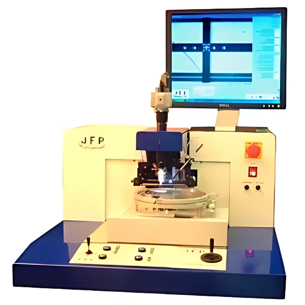
JFP Model S100 Dicing Saw

| Origin | France |
|---|---|
| Manufacturer Type | Authorized Distributor |
| Origin Category | Imported |
| Model | S100 |
| Price Range | USD 14,000 – 28,000 |
| Wafer Diameter | 76 mm (3″) |
| Minimum Die Size | 200 µm |
| Maximum Die Size | 10 mm × 10 mm |
| Wafer Thickness | ≥100 µm |
| Scribing Force Range | 3–50 gf (gram-force), motorized and programmable |
| Z-Axis Drive | Motorized, angle-adjustable |
| Diamond Blade | Adjustable tilt and rotational orientation |
| Tool Offset Calibration | Crosshair-aligned wafer stage |
| X/Y Positioning Resolution | 1 µm |
| Motion Control | Progressive joystick with fine-step increment |
| Optical Magnification | 1×–4× continuous zoom |
| Imaging System | 17″ TFT LCD monitor + high-definition color CCD camera |
| Illumination | Adjustable LED ring light |
| Scribing Speed (Y-axis) | 0.1–20 mm/sec, programmable |
| Scribe Length | User-defined, repeatable |
| Scribe Count per Program | Configurable |
| Break Mode | Operator-initiated or fully automated |
| Break Mechanism | Top-side polyester film + bottom-mounted mechanical cleaver |
| Film Handling | Removable, static-dissipative polyester tape |
| Alignment Method | Manual micrometer rotation (±90°), crosshair-based visual registration |
| Vacuum Requirement | 60% vacuum level |
| Compressed Air | 70 psi |
| Power Supply | 100–230 VAC, 50/60 Hz, 500 W |
| Dimensions (W×D×H) | 650 × 700 × 500 mm |
| Weight | 70 kg |
Ask about pricing, availability and specifications.
Overview
The JFP Model S100 Dicing Saw is a precision-engineered, semi-automated dicing system designed for controlled scribing and mechanical cleavage of compound semiconductor and silicon wafers up to 3 inches (76 mm) in diameter. Unlike abrasive sawing or laser-based separation methods, the S100 implements a non-contact scribing followed by controlled fracture process—leveraging established principles of micro-mechanical stress propagation and controlled crack initiation. This methodology preserves die edge integrity, minimizes chipping and subsurface damage, and eliminates thermal effects associated with laser ablation or plasma etching. The system is optimized for R&D laboratories, pilot-line fabrication facilities, and quality assurance environments where reproducible, low-contamination die separation is critical—particularly for GaAs, InP, SiC, and thin-silicon photonic devices.
Key Features
- Motorized Z-axis with programmable scribing force (3–50 gf), ensuring consistent line depth across variable material hardnesses and thicknesses.
- Angle-adjustable diamond scribing tool with independent rotational and tilt control, enabling optimization of kerf geometry and edge quality for anisotropic substrates.
- High-resolution XY stage (1 µm resolution) driven by stepper motors and controlled via progressive joystick, supporting both coarse navigation and sub-micron positioning repeatability.
- Integrated optical imaging subsystem comprising a continuously variable 1×–4× zoom objective, high-sensitivity color CCD camera, and 17″ TFT display—enabling real-time visual alignment, scribe path verification, and post-process inspection.
- Dual-mode cleavage architecture: operator-triggered or fully automated break sequence using top-side static-dissipative polyester film and synchronized bottom cleaver actuation—ensuring minimal lateral stress transfer to adjacent dies.
- Programmable scribe parameters including speed (0.1–20 mm/sec), length, repetition count, step indexing, touchdown velocity, and cleave timing—stored as reusable recipes for GLP-compliant workflow traceability.
Sample Compatibility & Compliance
The S100 accommodates standard 3-inch wafers with thicknesses ≥100 µm, including fragile substrates such as thinned SOI, GaAs epilayers, and MEMS-fabricated wafers. Its mechanical cleavage approach avoids particulate generation typical of diamond-blade dicing and eliminates organic residue common in UV-laser dicing. The system meets essential requirements for cleanroom-compatible operation (ISO Class 5 compatible with optional enclosure integration) and supports documentation protocols aligned with ISO/IEC 17025 and ASTM F2631–19 (Standard Practice for Semiconductor Wafer Dicing Process Qualification). Vacuum and pneumatic interfaces comply with ISO 8573-1 Class 3 compressed air specifications.
Software & Data Management
Operation is managed through a dedicated embedded controller with intuitive membrane keypad interface—no external PC required. All scribe and break parameters are stored in non-volatile memory with timestamped versioning. Optional RS-232 or USB-to-serial connectivity enables integration into lab-wide data acquisition networks. Audit trail functionality—including user ID logging, parameter change history, and execution timestamps—supports basic 21 CFR Part 11 readiness when paired with institutional electronic signature policies. Recipe export/import via USB flash drive facilitates cross-platform method transfer between instruments.
Applications
- R&D prototyping of optoelectronic chips (VCSELs, photodetectors, RF MMICs) requiring chip-level electrical and optical characterization prior to packaging.
- Pre-packaging singulation of MEMS sensors and microfluidic devices where edge contamination or residual stress must be avoided.
- Failure analysis sample preparation: precise isolation of suspect die without inducing secondary cracking or delamination.
- Academic and industrial thin-film device labs performing wafer-level process development for perovskite PV, flexible electronics, and 2D material heterostructures.
- Calibration and metrology labs requiring traceable, mechanically stable die separation for reference standard preparation.
FAQ
Is the S100 suitable for dicing ultra-thin wafers (<100 µm)?
No—the minimum supported wafer thickness is 100 µm. For thinner substrates, supplemental carrier bonding or temporary support films are required prior to scribing.
Can the system handle wafers with backside metallization or adhesive layers?
Yes, provided the metallization is non-reflective at visible wavelengths and does not interfere with optical alignment; adhesive residues must be fully cured and non-tacky to prevent film adhesion failure during cleavage.
What maintenance intervals are recommended for the diamond scribing tool?
Tool life depends on substrate hardness and cumulative scribe length; JFP recommends visual inspection after every 500 m of scribed line and replacement after 2,000 m or upon observed edge rounding under 4× magnification.
Does the S100 support automatic pattern recognition for die alignment?
No—it relies on manual crosshair-based visual alignment. Automated pattern recognition requires third-party machine vision integration via analog video output.
Is vacuum chuck flatness certified per ISO 10791-7?
The vacuum platen is manufactured to ≤2 µm total indicator reading (TIR) over 76 mm, verified during final factory calibration; full ISO 10791-7 certification is available upon request with additional metrology report.