Phenom Micro Electronics Insert for Desktop SEM
| Brand | Phenom |
|---|---|
| Origin | Netherlands |
| Manufacturer Type | Manufacturer |
| Origin Category | Imported |
| Model | Micro Electronics Insert |
| Price | Upon Request |
Overview
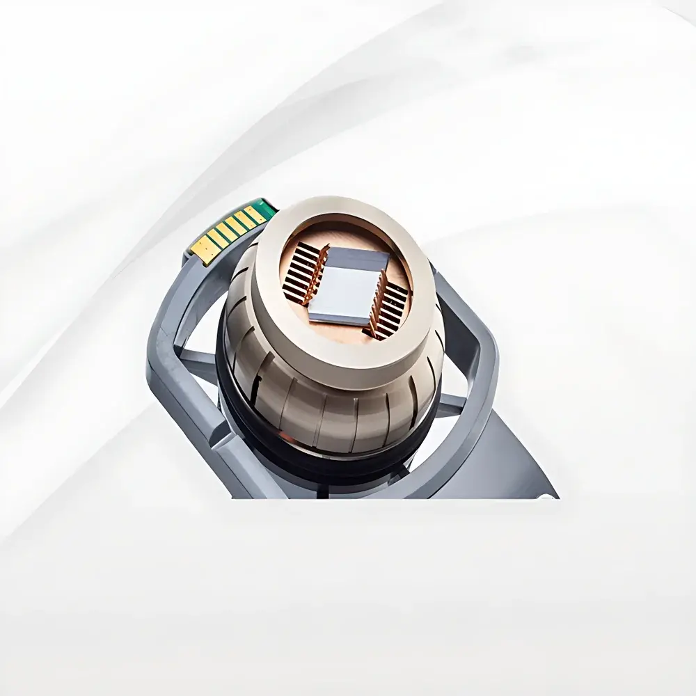
The Phenom Micro Electronics Insert is a purpose-engineered sample holder accessory designed exclusively for integration with Phenom desktop scanning electron microscopes (SEM). Unlike conventional stage adapters, this insert implements a non-contact, mechanical clamping principle based on precision-machined kinematic constraints and low-force spring-loaded retention—eliminating the need for conductive adhesives, carbon tape, or metal sputtering prior to imaging. Its operational principle leverages passive mechanical stabilization under vacuum conditions, ensuring minimal sample perturbation while maintaining electrical continuity through direct metal-to-metal contact at designated grounding points. This design is optimized for rapid, repeatable examination of delicate, high-value microelectronic components—including bare die, wire-bonded packages, photovoltaic cells, MEMS devices, and PCB interconnects—where surface integrity, charge dissipation control, and sub-10 µm feature visibility are critical.
Key Features
- Adhesive-free sample mounting: Eliminates carbon residue, outgassing artifacts, and thermal stress induced by curing tapes or silver paint.
- Kinematic sample positioning: Achieves sub-5 µm repeatability in X/Y/Z alignment across successive load cycles without recalibration.
- Compatibility with standard Phenom vacuum chamber geometry: Installs in <30 seconds via bayonet-style interface; no tooling or chamber venting required.
- Electrostatic discharge (ESD)-safe construction: All structural components meet ANSI/ESD S20.20 requirements; surface resistivity 10⁴–10⁶ Ω/sq.
- Height-tolerant clamping: Accommodates specimens up to 1.5 mm thick while maintaining parallelism within ±0.1° across the full 19 × 19 mm active area.
- Integrated grounding path: Direct copper-alloy contact points ensure stable charge drainage during high-current beam operation (up to 15 kV).
Sample Compatibility & Compliance
The Micro Electronics Insert supports flat, rigid specimens conforming to JEDEC J-STD-020 and IPC-7351 dimensional standards for surface-mount device (SMD) footprints. It is validated for use with silicon wafers (100–300 mm), diced die on dicing tape (with frame removal), thin-film solar cells (CIGS, perovskite), and flex circuit substrates (polyimide, LCP). The insert complies with ISO 14644-1 Class 5 cleanroom handling protocols when used with appropriate gloves and laminar flow hoods. No modification to the host Phenom system’s CE marking or IEC 61000-6-3 EMC certification is required upon installation.
Software & Data Management
Operation is fully transparent to Phenom’s proprietary Phenom Desktop Software (v5.2+). No driver installation or firmware update is necessary—the insert is auto-detected as a “Standard Stage Configuration” during system initialization. All acquired images retain native metadata including stage coordinates, working distance, and beam parameters. For regulated environments, the software supports audit-trail logging compliant with FDA 21 CFR Part 11 when deployed with network-authenticated user accounts and timestamped digital signatures. Image export formats include TIFF (16-bit linear), PNG, and CSV-based coordinate metadata for downstream CAD overlay or FA report generation.
Applications
- Fault isolation in failed IC packages using backside infrared (IR) contrast enhancement combined with secondary electron (SE) topography.
- Intermetallic compound (IMC) thickness assessment at Cu/Sn solder joints without cross-sectioning.
- Surface contamination mapping on photovoltaic cell electrodes via energy-dispersive X-ray spectroscopy (EDS) point analysis.
- Wire bond heel crack detection in power modules under low-kV (1–3 kV) landing energy to minimize charging artifacts.
- Qualification of laser-trimmed resistor networks on hybrid analog substrates.
FAQ
Does the Micro Electronics Insert require vacuum-compatible adhesives for high-vacuum mode?
No. The mechanical clamping mechanism functions reliably at base pressures down to 5 × 10⁻⁴ mbar without supplemental fixation.
Can it be used with EDS detectors on Phenom systems?
Yes. The insert’s low-Z aluminum alloy body produces negligible background X-ray interference; full-spectrum EDS quantification remains valid per ASTM E1508 guidelines.
Is thermal drift compensation supported during long-duration acquisition?
Drift correction is handled automatically by Phenom’s built-in image registration algorithm (SmartScan™); no hardware-level thermal compensation is embedded in the insert itself.
What cleaning protocol is recommended between samples?
Wipe contact surfaces with IPA-dampened lint-free wipes (e.g., Texwipe TX609); avoid ultrasonic cleaning due to potential spring fatigue.
Is calibration traceability provided with the insert?
Dimensional calibration is referenced to NIST-traceable gauge blocks used during manufacturing; a certificate of conformance (CoC) is supplied with each unit.


