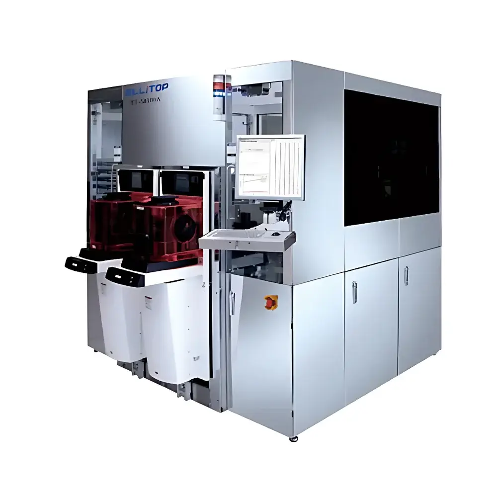
ELLITOP ET8100A Semiconductor Thin-Film Metrology System
| Brand | ELLITOP |
|---|---|
| Origin | Beijing, China |
| Model | ET8100A |
| Measurement Principle | Spectroscopic Ellipsometry (SE) + Spectral Reflectometry (SR) |
| Wafer Diameter Options | 100 mm, 150 mm, 200 mm, 300 mm |
| Substrate Thickness Range (measurable) | up to 2000 µm |
| Film Thickness Range | 0.1 nm – 120 µm |
| Homogeneous Film Thickness Range (substrate = film material) | 0.3 µm – 30 µm |
| Compliance | ASTM F1530, ISO/IEC 17025 (when configured per lab accreditation requirements), supports GLP/GMP data integrity workflows |
Overview
The ELLITOP ET8100A Semiconductor Thin-Film Metrology System is an integrated optical metrology platform engineered for high-precision, non-contact characterization of dielectric and semiconductor thin films during front-end and back-end process development and high-volume manufacturing. It combines spectroscopic ellipsometry (SE) and spectral reflectometry (SR) in a single instrument architecture—enabling simultaneous acquisition of complex refractive index (n, k), layer thickness, interface roughness, and compositional gradients across single-layer and multilayer stacks. Unlike standalone reflectometers or conventional ellipsometers, the ET8100A leverages dual-optical-path synchronization and real-time spectral deconvolution to resolve sub-nanometer thickness variations on patterned and unpatterned wafers, with particular robustness on low-k dielectrics, high-k gate oxides, epitaxial SiC/GaN layers, and ultra-thin ALD-deposited films. Its modular optical head design accommodates variable incident angles and polarization states, ensuring measurement fidelity across diverse film-substrate combinations—including transparent, semi-transparent, and absorbing systems.
Key Features
- Dual-mode optical engine: Simultaneous SE/SR data acquisition over 190–1700 nm spectral range, enabling cross-validated modeling and reduced parameter correlation in multi-layer fitting.
- Configurable wafer handling: Motorized XYZ stage with optional auto-loading, edge-detection alignment, and OCR-based wafer ID recognition compliant with SEMI E142 standards.
- Material-agnostic substrate support: Validated for Si, SiC, GaN, quartz, fused silica, sapphire, GaAs, and glass substrates—regardless of transparency, conductivity, or crystallinity.
- Homogeneous film capability: Unique calibration protocol for same-material film/substrate systems (e.g., Si-on-Si, SiO₂-on-SiO₂), resolving thickness from 0.3 µm to 30 µm with <±0.2% repeatability (1σ, n≥30).
- Modular expansion interfaces: Dedicated ports for optional modules including wafer warpage mapping (via interferometric topography), resistivity profiling (with four-point probe integration), and spatially resolved stress analysis.
Sample Compatibility & Compliance
The ET8100A supports full-wafer and site-specific measurements on bare, oxidized, nitrided, or metallized wafers—without requiring vacuum or surface preparation. It meets critical industry traceability requirements: raw spectral data and model parameters are timestamped, user-annotated, and stored with immutable audit trails. When deployed in regulated environments, the system can be configured to comply with FDA 21 CFR Part 11 (electronic records/signatures), ISO/IEC 17025 clause 7.7 (result reporting), and ASTM F1530-22 (standard guide for ellipsometric measurement of thin films). All calibration references are NIST-traceable via certified SRM 2036 (silicon oxide thickness standards) and custom-fabricated Si/SiO₂/NiCr reference wafers.
Software & Data Management
Controlled by ELLITOP’s MetroSuite™ v4.x software, the ET8100A provides a deterministic workflow from measurement setup to statistical process control (SPC) export. The software features physics-based optical modeling using rigorous coupled-wave analysis (RCWA) for grating structures and effective medium approximation (EMA) for porous or graded layers. All models are saved as XML-based project files with embedded metadata (instrument configuration, environmental conditions, operator ID). Data exports conform to SEMI E132 (XML-based metrology data format) and support direct integration into factory host systems (MES/AMHS) via OPC UA or flat-file FTP. Audit logs record every parameter change, model revision, and report generation event—fully supporting GLP and GMP validation protocols.
Applications
- Gate oxide and high-k dielectric thickness uniformity monitoring in CMOS and FinFET fabrication.
- ALD/CVD process control for TiN, TaN, HfO₂, and LaAlO₃ films on 300 mm wafers.
- Epitaxial layer thickness and doping profile estimation in SiC power device epitaxy.
- Post-CMP thickness verification of low-k ILD stacks with embedded metal lines.
- Development of optical constants databases for novel 2D materials (MoS₂, h-BN) and perovskite thin films.
FAQ
Does the ET8100A require vacuum operation for ellipsometry measurements?
No—measurements are performed in ambient air; nitrogen purging is optional for UV-range stability below 220 nm.
Can the system measure films on patterned wafers with dense line/space features?
Yes—through RCWA-enabled modeling and spot-size optimization down to 25 µm diameter.
Is remote diagnostics and firmware update supported?
Yes—MetroSuite™ includes secure TLS-encrypted remote access with role-based permissions and version-controlled update deployment.
What level of training and application support is provided?
ELLITOP offers on-site installation qualification (IQ), operational qualification (OQ), and application-specific model development workshops led by PhD-level metrology engineers.
How is measurement uncertainty quantified and reported?
Each measurement includes a full covariance matrix output; combined standard uncertainty (k=2) is calculated per GUM (JCGM 100:2018) and reported alongside thickness and n/k values.