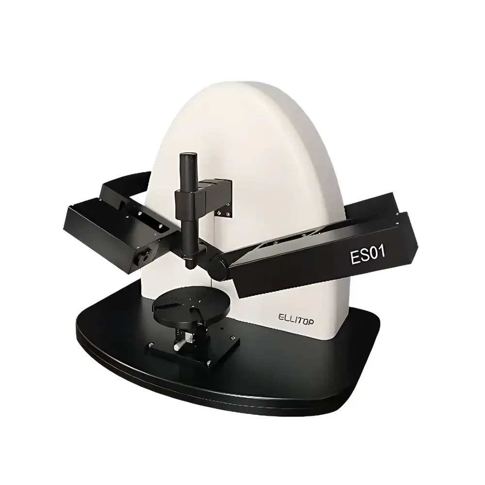
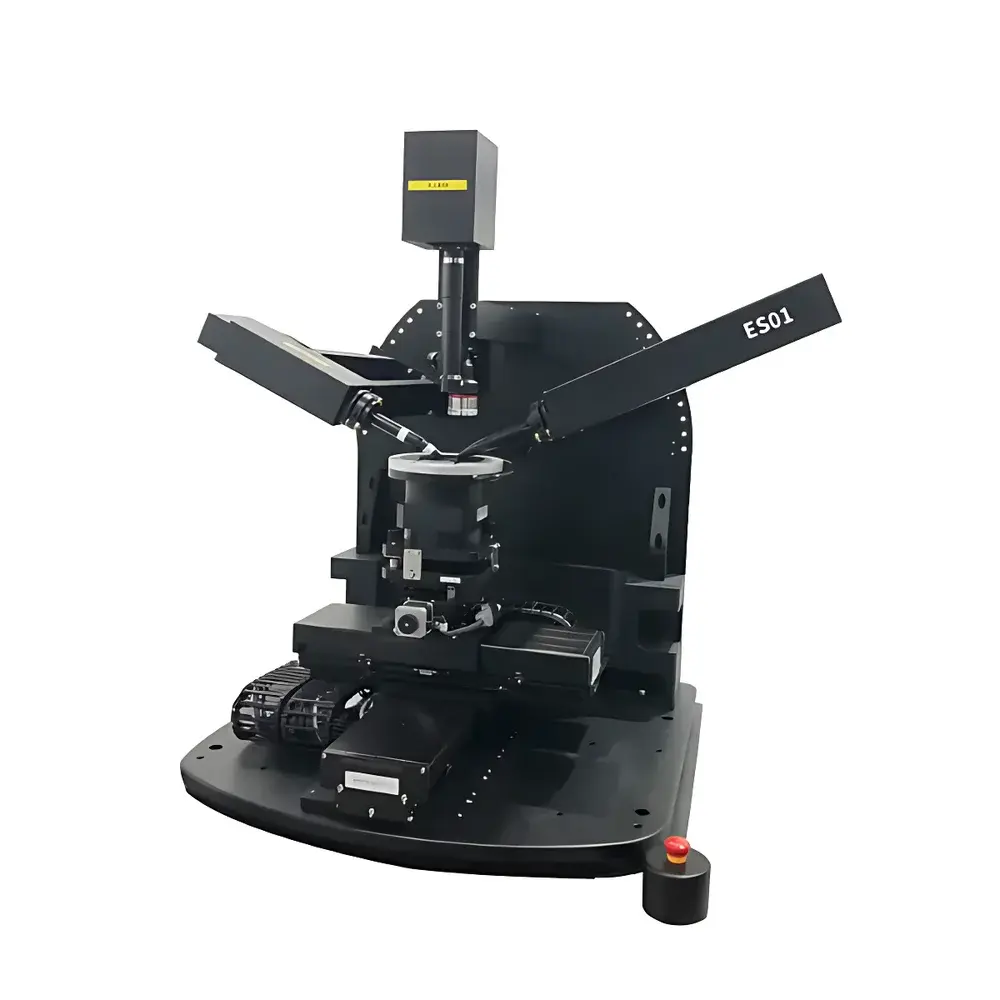
ELLITOP ES01 Spectroscopic Ellipsometer
| Brand | ELLITOP |
|---|---|
| Origin | Beijing, China |
| Manufacturer Type | Authorized Distributor |
| Model | ES01 |
| Spectral Range | 190–25000 nm |
| Spot Size | Manually adjustable from 1–5 mm |
| Angle of Incidence | (A) Motorized variable: 30°–90° |
| (M) Manual variable | 40°–90° |
| Measurement Speed | ≤0.05 s per spectrum (fastest) |
| Single Measurement Time | 1–2 s |
| Sample Compatibility | Supports 4″, 6″, 8″, and 12″ wafers (custom substrates available) |
| Spectral Resolution | ≤0.45 nm (190–1000 nm), ≤3.5 nm (1000–1700 nm), ≤7 nm (1700–2500 nm) |
| Thickness Accuracy | ≤0.4 nm (measured on 100 nm SiO₂ on Si reference standard) |
| Thickness Repeatability | ±0.005 nm |
| Refractive Index Repeatability | ±0.0002 |
| Direct Beam Accuracy | Ψ = 45° ±0.075°, Δ = 0° ±0.05° (10 s averaging, ≥95% of spectral range) |
Overview
The ELLITOP ES01 Spectroscopic Ellipsometer is a high-precision, rapid-acquisition optical metrology instrument engineered for quantitative characterization of thin-film nanostructures and bulk optical materials. Operating on the fundamental principles of spectroscopic ellipsometry—where polarized light reflects from or transmits through a sample and induces measurable changes in its amplitude ratio (Ψ) and phase difference (Δ)—the ES01 delivers non-contact, non-destructive, and model-based determination of film thickness, complex refractive index (n + ik), dielectric function components (ε₁, ε₂), and surface optical anisotropy. Its broad spectral coverage—from deep ultraviolet (190 nm) through visible and near-infrared to mid-infrared (25,000 nm)—enables comprehensive dispersion analysis across technologically critical material systems, including dielectrics (SiO₂, HfO₂), semiconductors (Si, Ge, GaAs), 2D materials (graphene, MoS₂), transparent conductive oxides (ITO, AZO), and organic thin films. The system employs a rotating compensator configuration, ensuring full 0°–360° Δ measurement without ambiguity or dead zones, while inherently mitigating depolarization artifacts induced by surface roughness or subsurface scattering.
Key Features
- Rotating Compensator Architecture: Enables unambiguous, high-fidelity Ψ and Δ acquisition across the full angular and spectral range—critical for modeling anisotropic, graded, or ultra-thin (<1 nm) layers with atomic-layer sensitivity.
- Sub-50-ms Full-Spectrum Acquisition: Achieves ≤0.05 s per spectrum under optimized conditions, supporting real-time process monitoring and high-throughput R&D screening.
- Micro-Spot Capability: Adjustable spot size down to ≤30 µm enables spatially resolved mapping of patterned wafers, MEMS devices, and heterogeneous thin-film stacks.
- Multi-Angle Flexibility: Motorized (30°–90°) and manual (40°–90°) incidence angle options enhance measurement robustness for low-contrast films, absorbing substrates, or multilayer interference-limited configurations.
- Integrated Video Alignment System: High-resolution coaxial imaging ensures precise positioning relative to fiducials or device features—reducing operator-induced alignment error and enabling repeatable site-specific metrology.
- Unified Optical Characterization: Simultaneous acquisition of Ψ/Δ, Mueller matrix elements (12 independent parameters), depolarization coefficient, reflectance (R), and transmittance (T) within a single measurement sequence.
- One-Click Workflow Automation: Preconfigured routines for measurement, optical modeling, regression fitting, and report generation streamline operation—while open-access scripting and extensible material/database libraries support advanced research protocols.
Sample Compatibility & Compliance
The ES01 accommodates industry-standard semiconductor wafers (4″ to 12″), glass substrates, flexible polymer films, and custom-shaped samples via modular stage design. Its mechanical and optical architecture complies with ISO 9001-aligned manufacturing practices, and measurement traceability is maintained through NIST-traceable calibration standards (e.g., Si/SiO₂ reference wafers). While not pre-certified for regulated environments, the system supports GLP/GMP-compliant workflows via optional audit trail logging, user access control, and electronic signature modules compatible with FDA 21 CFR Part 11 requirements. All optical models adhere to established physical optics conventions defined in ASTM E1933 (Standard Practice for Spectroscopic Ellipsometry) and ISO 15630-3 (Optical methods for thin-film thickness measurement).
Software & Data Management
Built on a modular, Windows-based platform, the ES01 software suite includes EllipsoFit™—a physics-driven modeling engine supporting layered, gradient, effective medium, and anisotropic optical models. It integrates over 300 built-in material dispersion models (Cauchy, Sellmeier, Tauc-Lorentz, Cody-Lorentz) and allows user-defined dielectric functions. Raw data (Ψ, Δ, R, T, Mueller elements) are stored in HDF5 format with embedded metadata (wavelength, angle, date/time, instrument ID, operator). Export options include CSV, XML, and industry-standard JADE-compatible formats for third-party analysis. Version-controlled project files ensure reproducibility, and batch processing enables automated analysis across wafer maps or time-series datasets.
Applications
- Atomic-layer deposition (ALD) and chemical vapor deposition (CVD) process development and endpoint detection
- Optical coating design validation (anti-reflective, high-reflection, filter stacks)
- Characterization of 2D materials and van der Waals heterostructures
- Quality control of photovoltaic absorber layers (CIGS, perovskites, a-Si)
- Determination of carrier concentration and mobility in doped semiconductors via Drude-Lorentz modeling
- In-line metrology for display TFT backplanes (IGZO, LTPS) and OLED encapsulation layers
- Biomedical thin-film sensing (hydrogel swelling, protein adsorption kinetics)
FAQ
What spectral resolution does the ES01 achieve across its full range?
The system delivers ≤0.45 nm resolution from 190–1000 nm, ≤3.5 nm from 1000–1700 nm, and ≤7 nm from 1700–25000 nm—optimized for signal-to-noise balance and measurement speed.
Can the ES01 measure transparent conductive oxides like ITO on glass?
Yes—the combination of UV–Vis–NIR coverage and rotating compensator stability enables accurate n/k extraction and thickness quantification for TCOs, even at sub-50 nm thicknesses.
Is Mueller matrix measurement included in standard configuration?
Yes—full 3×4 Mueller matrix acquisition is enabled by default, supporting generalized ellipsometry and depolarization analysis without hardware modification.
Does the system support automated wafer mapping?
With optional motorized XY stages and programmable scripting, the ES01 supports coordinate-based multi-site measurements and exportable map files for overlay with lithography or defect inspection tools.
How is measurement accuracy validated?
Factory calibration uses certified Si/SiO₂ reference standards traceable to national metrology institutes; users may perform periodic verification using in-house reference wafers with documented thickness and optical constants.