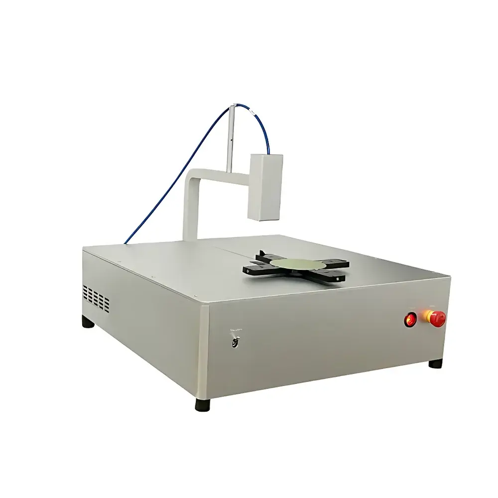
ELLITOP EH100-X White Light Interferometric Thickness Measurement System
| Brand | ELLITOP |
|---|---|
| Origin | Beijing, China |
| Model | EH100-X |
| Wavelength Range | 190–1700 nm |
Overview
The ELLITOP EH100-X White Light Interferometric Thickness Measurement System is an optical metrology instrument engineered for non-contact, high-precision determination of thin-film thickness and surface topography on transparent, semi-transparent, and reflective substrates. It operates on the principle of spectral-domain white light interferometry (WLI), where broadband interference fringes generated from multiple optical interfaces—such as air/film and film/substrate—are captured by a spectrometer and analyzed via Fourier-transform-based algorithms to extract film thickness with sub-nanometer resolution. Unlike stylus profilometers or ellipsometers, the EH100-X requires no physical contact, eliminates sample damage risk, and delivers rapid, repeatable measurements across wafer-scale or discrete substrates without calibration drift. Its broad spectral coverage (190–1700 nm) enables robust characterization of multi-layer stacks, including UV-curable resists, wide-bandgap dielectrics (e.g., SiO₂, Si₃N₄), low-k polymers, and conductive oxides (e.g., ITO), making it suitable for both R&D labs and inline process monitoring environments.
Key Features
- Non-destructive, non-contact measurement based on spectral white light interferometry
- Simultaneous acquisition of film thickness, optical constants (n, k), and surface roughness (Ra, Rq)
- Extended wavelength range from deep ultraviolet (190 nm) to near-infrared (1700 nm), supporting analysis of ultra-thin (10 µm) films
- Automated stage positioning with optional motorized XYZ translation and rotation for mapping large-area samples (up to 200 mm wafers)
- Integrated high-sensitivity CCD spectrometer with thermoelectric cooling for low-noise spectral acquisition
- Modular optical design compatible with standard microscope objectives (5× to 100×) and custom illumination geometries (normal incidence or variable-angle)
- Robust architecture compliant with ISO 9001-certified manufacturing processes; designed for 24/7 operation in cleanroom-class environments (ISO Class 5 or better)
Sample Compatibility & Compliance
The EH100-X accommodates rigid and flexible substrates including silicon wafers, fused silica, sapphire, glass (soda-lime, borosilicate), PET, PI, and metal foils. It supports single-layer and multi-layer film systems—whether isotropic or anisotropic—with no requirement for prior knowledge of refractive index. The system meets key industry-relevant compliance frameworks: spectral data acquisition adheres to ASTM E2843 (Standard Guide for Spectral Reflectance Measurements), thickness reporting aligns with SEMI MF1530 (Test Method for Optical Measurement of Thin-Film Thickness), and software audit trails support GLP/GMP documentation requirements per FDA 21 CFR Part 11 when configured with user authentication and electronic signature modules. All firmware and calibration protocols are traceable to NIST-traceable reference standards.
Software & Data Management
The EH100-X is operated via ELLITOP’s proprietary Thickness Analysis Suite (TAS v4.x), a Windows-based application offering real-time spectral visualization, multi-layer modeling (up to 10 layers), and automatic peak detection with confidence interval estimation. Data export formats include CSV, XML, and HDF5 for integration into MES, SPC, or LIMS platforms. The software supports batch processing, recipe-driven measurement sequences, and statistical process control (SPC) charting with Cp/Cpk calculation. Audit logs record operator ID, timestamp, instrument configuration, raw spectra, and final thickness values—enabling full traceability during regulatory inspections. Optional cloud synchronization allows secure remote access to historical datasets and cross-site comparison reports.
Applications
- Semiconductor fabrication: thickness uniformity mapping of photoresists, gate oxides, hard masks, and barrier layers post-CMP or PVD/CVD deposition
- Flat-panel display manufacturing: quantification of TFT stack layers (a-Si, SiNx, ITO), OLED emissive/transport layers (NPB, PVK, PEDOT:PSS), and encapsulation films
- Optical coating development: verification of anti-reflective, high-reflection, and bandpass filter designs on lenses, mirrors, and laser components
- Functional coatings: evaluation of self-cleaning TiO₂, electrochromic WO₃, and hydrophobic SiO₂-based nanocomposites
- Flexible electronics: thickness and homogeneity assessment of transparent conductive films (Ag nanowire, graphene oxide, conductive polymers) on PET or PI substrates
- Academic research: in-situ monitoring of spin-coating dynamics, solvent evaporation kinetics, and interfacial diffusion in polymer bilayers
FAQ
What film thickness range can the EH100-X measure?
The system measures films from <1 nm (e.g., native oxide on Si) up to ~10 µm (e.g., thick polymer resist), depending on material dispersion and substrate reflectivity.
Does it require vacuum or inert atmosphere operation?
No—measurements are performed under ambient conditions; optional environmental chamber integration supports controlled temperature/humidity testing.
Can it analyze rough or patterned surfaces?
Yes, with appropriate objective selection and algorithmic deconvolution of topographic contributions from optical path differences.
Is training and technical support available internationally?
ELLITOP provides remote commissioning, application-specific training webinars, and on-site service through authorized regional partners in North America, Europe, and APAC.
How often does the system require recalibration?
Factory calibration is stable for ≥12 months under normal use; annual verification using NIST-traceable thickness standards is recommended for ISO/IEC 17025 compliance.