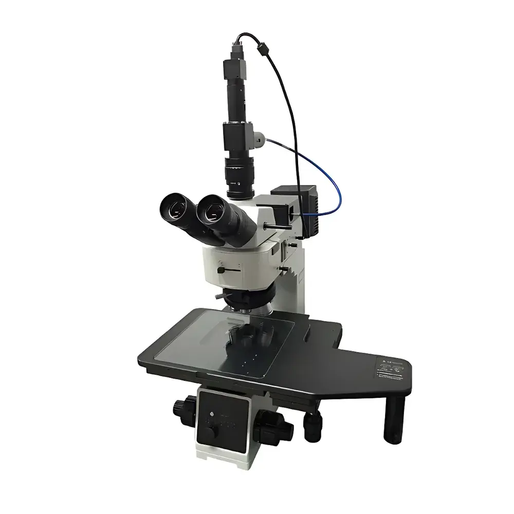
ELLITOP EH300 White Light Interferometric Micro-Thickness Measurement System
| Brand | ELLITOP (Beijing Ellitop Technology Co., Ltd.) |
|---|---|
| Origin | Beijing, China |
| Model | EH300 |
| Wavelength Range | 380–800 nm |
| Thickness Measurement Range | 0.05 µm – 50 µm |
| Measurement Accuracy | ±2 nm or ±0.2% of reading (whichever is greater) |
Overview
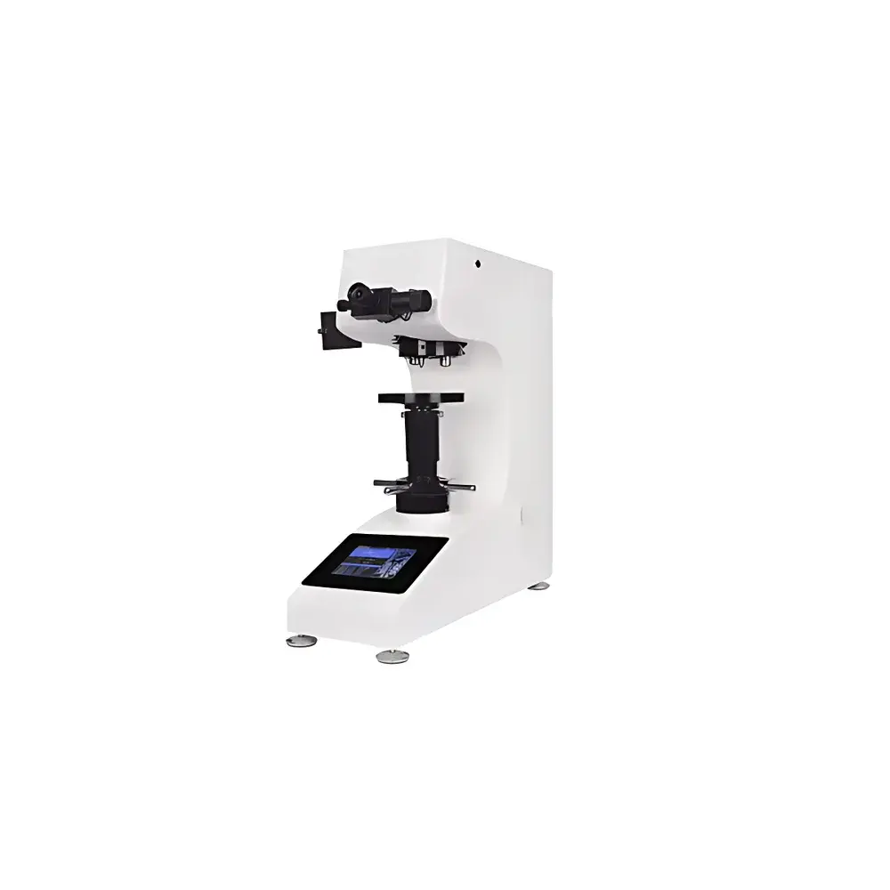
The ELLITOP EH300 White Light Interferometric Micro-Thickness Measurement System is a non-contact, high-resolution optical metrology instrument engineered for precise thickness characterization of thin films and multilayer structures at the microscale. It operates on the principle of spectral-domain white light interferometry (WLI), combining collimated broadband illumination (380–800 nm) with high-magnification microscopic imaging. When vertically incident light reflects from both the top surface of a thin film and its underlying substrate interface, interference fringes are generated in the spectral domain. The system captures the resulting reflectance spectrum and reconstructs film thickness through inverse modeling based on Fresnel equations and thin-film optical theory. Unlike stylus profilometry or ellipsometry, the EH300 requires no physical contact, eliminates sample damage risk, and delivers quantitative layer-thickness data—even for transparent, semi-transparent, or weakly absorbing films—within sub-second acquisition times. Its integrated microscope platform enables spatially resolved measurements across user-defined micro-regions (down to ~1 µm lateral resolution, dependent on objective magnification), making it suitable for R&D labs and production environments where localized process control is critical.
Key Features
- Micro-region targeting capability with interchangeable high-NA microscope objectives (3×, 5×, 10×, 20×, 50× options) for flexible field-of-view and resolution selection
- Integrated visual optical path with coaxial eyepiece viewing system for rapid manual identification and alignment of measurement sites
- Manual precision stage with clutch-enabled coarse translation, enabling fast positioning across full travel range without compromising fine adjustment fidelity
- Coaxial coarse/fine focusing mechanism with anti-slip design, positioned at low-hand ergonomic height for extended operator comfort and repeatability
- Real-time FFT-accelerated spectral analysis engine—typical single-point measurement completed in ≤1 second
- Brightfield/darkfield illumination toggle for enhanced contrast in heterogeneous or low-reflectivity samples
- Optional metallurgical configuration supporting reflected-light microstructure observation (e.g., grain boundary, phase distribution) alongside thickness mapping
- Robust mechanical architecture optimized for stability under ambient laboratory or light industrial conditions
Sample Compatibility & Compliance
The EH300 accommodates rigid and planar substrates including silicon wafers, glass, quartz, sapphire, metal foils, and polymer films. It supports single-layer and multi-layer stack analysis—provided optical constants (n, k) of constituent materials are known or can be approximated from reference databases. Applications span semiconductor fabrication (photoresist, SiO₂, SiNₓ, low-k dielectrics), flat-panel display manufacturing (ITO, AlQ₃, PEDOT:PSS, polyimide), optical coating QC (AR, HR, bandpass filters), and functional polymer development (hydrophobic, electrochromic, barrier layers). While not certified to ISO/IEC 17025 or ASTM E2942 per se, the system’s measurement traceability aligns with NIST-traceable spectral radiometry practices. Data acquisition logs include timestamp, operator ID, instrument configuration, and environmental metadata—supporting GLP-compliant documentation workflows.
Software & Data Management
The proprietary EH300 Control & Analysis Suite runs on Windows OS and provides intuitive point-and-click operation. Core modules include real-time spectrum visualization, automated peak search, multi-layer fitting with constraint-based optimization, cross-sectional thickness profiling, and export-ready reporting (CSV, PDF, PNG). All measurement sessions generate immutable audit trails containing raw interferograms, fitted parameters, confidence intervals, and user annotations. Software supports 21 CFR Part 11–compatible electronic signatures when deployed with validated IT infrastructure. Batch processing mode enables unattended sequential measurements across predefined coordinate grids—ideal for wafer-level uniformity mapping. Export formats integrate seamlessly with statistical process control (SPC) platforms and LIMS systems.
Applications
- Semiconductor process monitoring: photoresist spin-coating uniformity, post-CMP oxide thickness variation, PVD/CVD stack integrity verification
- Display technology R&D: organic emissive layer (e.g., NPB, PVK) thickness control in OLED backplanes; gate dielectric (SiNₓ) thickness in TFT arrays
- Optical component manufacturing: anti-reflective coating thickness validation on lenses and laser optics; durability assessment of hard coatings on polycarbonate substrates
- Advanced packaging: conformal encapsulation layer thickness on MEMS devices; under-bump metallization (UBM) stack analysis
- Academic research: sol-gel derived thin film growth kinetics; Langmuir-Blodgett monolayer quantification; 2D material flake thickness screening
FAQ
What types of films can the EH300 measure?
It measures transparent, semi-transparent, and weakly absorbing dielectric and organic films on reflective or semi-reflective substrates—including oxides, nitrides, polymers, photoresists, and small-molecule organics.
Is calibration required before each measurement?
No routine recalibration is needed; the system uses built-in reference spectra and factory-characterized optical path delays. A single baseline correction is recommended after major environmental shifts (e.g., >5°C temperature change or optical component replacement).
Can the EH300 be integrated into an automated production line?
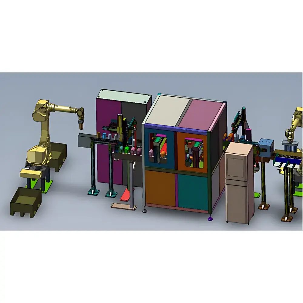
Yes—via Ethernet-based remote command protocol (TCP/IP) and programmable API support, enabling synchronization with robotic handlers and MES systems for inline SPC deployment.
Does the software support multi-layer thickness deconvolution?
Yes—up to four-layer models are supported with user-definable optical constants, layer sequence, and interface roughness constraints.
What is the minimum measurable spot size?
Dependent on objective choice: ~1.2 µm (with 50× objective, NA=0.55) under optimal focus and signal-to-noise conditions.