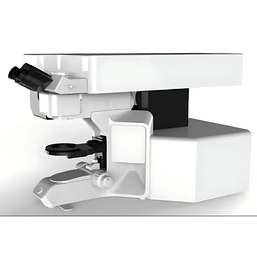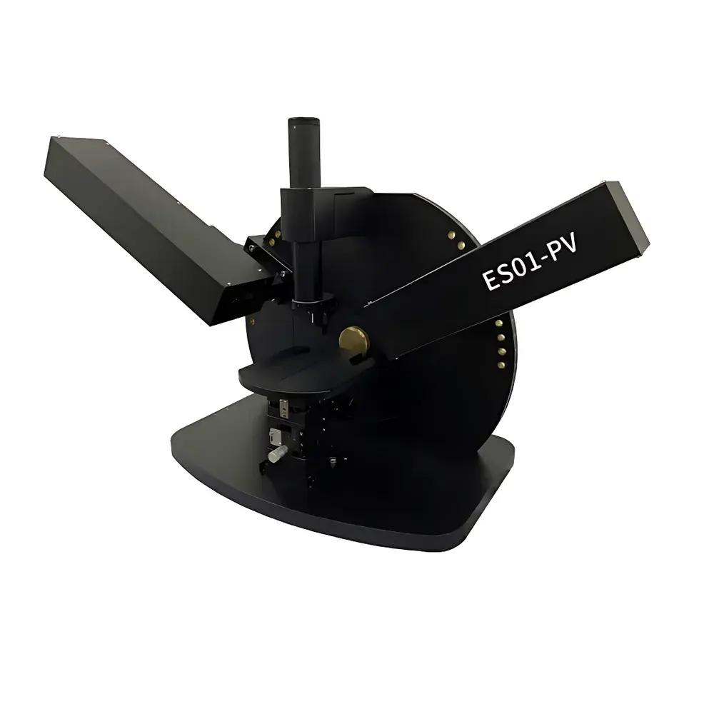
ELLITOP ES01-PV Spectroscopic Ellipsometer
| Brand | ELLITOP |
|---|---|
| Origin | Beijing, China |
| Model | ES01-PV |
| Spectral Range | 245–1000 nm (UV-Vis-NIR) |
| Spot Size | Manually adjustable, 1–4 mm diameter |
| Angle of Incidence | Manually adjustable, 40°–90° in 5° increments, repeatability ±0.02° |
| Single Measurement Time | 5–10 s for full Ψ/Δ spectrum acquisition |
Overview
The ELLITOP ES01-PV Spectroscopic Ellipsometer is a purpose-built metrology instrument engineered for high-precision characterization of nanostructured thin films in photovoltaic (PV) R&D and manufacturing quality control. Operating on the fundamental principles of spectroscopic ellipsometry—measuring the change in polarization state (Ψ and Δ) of reflected light across a broad spectral range—the ES01-PV delivers quantitative optical constants (refractive index n, extinction coefficient k) and geometric parameters (layer thickness, roughness, interface grading) of multilayer stacks on textured silicon substrates. Its 245–1000 nm spectral coverage spans deep ultraviolet through near-infrared, enabling robust modeling of critical passivation layers—including Al₂O₃, SiNx, SiO₂, TiO₂, and their combinations—on PERC, TOPCon, heterojunction (HJT), and IBC solar cells. Unlike conventional ellipsometers optimized for flat wafers, the ES01-PV integrates hardware and software innovations specifically to address the metrological challenges of low-reflectance, highly scattering, and topographically complex textured surfaces.
Key Features
- Rotating compensator architecture with full 0–360° Δ measurement capability, eliminating null-point ambiguity and mitigating depolarization artifacts induced by surface roughness
- High-sensitivity detection module optimized for low-reflectance (<10%) textured silicon substrates, incorporating broadband achromatic compensation and multi-quadrant error suppression
- Manual incidence angle adjustment from 40° to 90° in precise 5° steps, with angular repeatability better than ±0.02°, supporting multi-angle data acquisition for enhanced model uniqueness
- Adjustable probe spot size (1–4 mm diameter) to accommodate localized analysis on patterned or non-uniform samples without compromising signal integrity
- Full-spectrum Ψ/Δ acquisition completed in 5–10 seconds, enabling rapid process feedback during inline or lab-based QC workflows
- Sub-nanometer thickness resolution (≤0.05 nm) validated on standard SiO₂/Si reference structures under controlled environmental conditions
- Integrated video alignment system with real-time magnified imaging, ensuring accurate positioning over micro-textured regions and minimizing operator-induced misalignment
- One-click measurement-to-analysis workflow via ETES software, automating optical modeling, regression fitting, and uncertainty estimation
Sample Compatibility & Compliance
The ES01-PV is validated for use with crystalline silicon wafers featuring pyramidal, random, or planar textures, as well as planar dielectric and semiconductor thin-film stacks. It supports direct measurement of single-layer antireflection coatings (e.g., SiNx, Al₂O₃), dual-layer stacks (e.g., SiNx/SiO₂, SiNx/Al₂O₃), and graded interfacial layers common in advanced passivation schemes. While not certified to ISO/IEC 17025 or ASTM E1938, the instrument’s measurement traceability follows established ellipsometric calibration protocols using NIST-traceable Si/SiO₂ reference standards. Data output complies with ASTM F2687 (Standard Practice for Spectroscopic Ellipsometry Calibration) and supports GLP-compliant documentation when integrated with laboratory information management systems (LIMS).
Software & Data Management
ETES (ELLITOP Ellipsometry Software) provides a modular, wizard-driven interface for both novice and expert users. Core functionalities include automated optical model construction, library-based material dispersion fitting (Cauchy, Tauc-Lorentz, Cody-Lorentz), and constrained multi-angle regression. The software embeds preconfigured application templates for PV-specific layer systems—such as Al₂O₃/SiNx/c-Si—and includes an extensible materials database containing >120 experimentally validated optical constants for semiconductors, dielectrics, and metals. All measurement sessions log raw Ψ/Δ spectra, fitted parameters, covariance matrices, and residual error maps. Export formats include CSV, XML, and HDF5, facilitating integration with MATLAB, Python (NumPy/SciPy), and statistical process control (SPC) platforms. Audit trails record user actions, parameter changes, and fit convergence history per measurement, aligning with FDA 21 CFR Part 11 requirements when deployed on validated Windows OS environments.
Applications
- Thickness and optical constant mapping of atomic-layer-deposited (ALD) Al₂O₃ passivation films on textured c-Si
- Quantitative analysis of SiNx film stoichiometry (Si/N ratio) via dispersion modeling in the 300–800 nm range
- Interfacial oxide thickness estimation beneath SiNx layers in TOPCon cell architectures
- In-line monitoring of PECVD SiNx deposition uniformity across 156–210 mm wafers
- Optical characterization of transparent conductive oxides (TCOs) such as ITO and ZnO in bifacial cell designs
- Reference-free determination of complex refractive index of bulk silicon wafers, including carrier concentration effects in the NIR
FAQ
What sample preparation is required prior to measurement?
No special preparation is needed beyond standard wafer cleaning (RCA or piranha). Textured surfaces are measured directly; no flattening or polishing is required.
Can the ES01-PV measure films on metal substrates?
Yes, but with reduced sensitivity for ultra-thin (<2 nm) dielectric layers due to strong substrate absorption; modeling requires inclusion of appropriate metal dielectric functions.
Is vacuum or inert atmosphere operation supported?
No—the system operates under ambient laboratory conditions. For air-sensitive samples, optional nitrogen purge accessories are available upon request.
How is measurement reproducibility verified?
Repeatability is assessed using NIST-traceable Si/SiO₂ reference wafers measured daily; typical 3σ thickness variation is ≤0.1 nm for 100 nm SiO₂ layers.
Does ETES support scripting or API access for automation?
Yes—ETES exposes a COM interface compatible with VB.NET, C#, and Python (via pywin32), enabling integration into automated test sequences and factory MES systems.