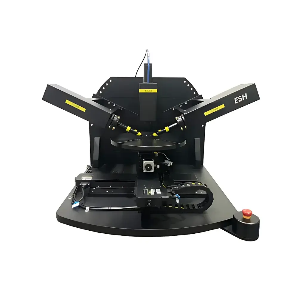
ELLITOP ESH Series Spectroscopic Ellipsometer
| Brand | ELLITOP |
|---|---|
| Origin | Beijing, China |
| Model | ESH |
| Spectral Range | 190–2500 nm (customizable) |
| Spot Size | ≤200 µm (customizable, down to 1 µm) |
| Angle of Incidence | Motorized auto-adjustment from 30° to 90° |
| manual fine-tuning range | 40°–90° |
| Single-Measurement Time | 3–5 s (full spectrum) |
| Sample Compatibility | Supports 150 mm (6″), 200 mm (8″), and 300 mm (12″) wafers |
| Measurement Capability | Nanoscale film thickness (sub-Å resolution), complex refractive index (n, k), dielectric function (ε₁, ε₂), bulk optical constants |
Overview
The ELLITOP ESH Series Spectroscopic Ellipsometer is a high-precision, research-grade optical metrology instrument engineered for non-destructive, contactless characterization of thin-film and bulk material optical properties. It operates on the fundamental principle of spectroscopic ellipsometry—measuring the change in polarization state (Δ and Ψ) of light reflected from a sample surface across a broad spectral range. By modeling the optical response using rigorous multilayer optical theory (e.g., Fresnel equations with transfer-matrix formalism), the ESH extracts critical nanoscale structural and electronic parameters—including film thickness (from sub-angstrom to >100 µm), complex refractive index (n + ik), extinction coefficient (k), and full dielectric function components (ε₁, ε₂). Its 190–2500 nm spectral coverage enables comprehensive analysis across UV-VIS-NIR regimes, supporting applications ranging from atomic-layer-deposited (ALD) gate oxides to thick polymer coatings and photonic crystal structures.
Key Features
- Rotating Compensator Architecture: Utilizes a photoelastic modulator (PEM)-based rotating compensator design for high-accuracy, rapid acquisition of the full Stokes vector without moving parts in the detection path—ensuring long-term stability and minimal drift.
- Sub-Micron Spatial Resolution: Achieves spot sizes down to 1 µm via precision micro-optics and motorized focusing, enabling localized mapping of patterned wafers, device cross-sections, and heterogeneous surfaces.
- Multi-Angle Flexibility: Combines motorized incidence angle control (30°–90°) with programmable presets (60°, 65°, 70°) and manual fine adjustment (40°–90°), optimizing sensitivity for specific layer stacks and minimizing correlation between fitted parameters.
- Video-Assisted Alignment: Integrated high-resolution coaxial microscope with real-time video feed and crosshair overlay ensures precise positioning on features as small as 5 µm—critical for process control in semiconductor fab environments.
- Sub-Second Spectral Acquisition: Full-spectrum measurement completed in ≤5 seconds per point, enabling high-throughput mapping (e.g., 300-point wafer scan in 10⁴).
- One-Touch Workflow: Intuitive GUI-guided measurement sequences—from alignment and calibration to model building and real-time fitting—reduce operator dependency and support unattended operation in GLP/GMP-compliant labs.
Sample Compatibility & Compliance
The ESH accommodates standard semiconductor substrates including 150 mm (6″), 200 mm (8″), and 300 mm (12″) silicon, sapphire, or compound semiconductor wafers. Vacuum-compatible and temperature-controlled stage options are available for in-situ process monitoring. All hardware and software modules comply with ISO/IEC 17025 requirements for calibration traceability. Data acquisition and reporting adhere to FDA 21 CFR Part 11 guidelines when configured with audit-trail-enabled software licenses, supporting regulated environments in pharmaceutical thin-film development and medical device coating QC.
Software & Data Management
The proprietary ELLITOP Analysis Suite provides a modular, scriptable platform for optical modeling, regression analysis, and statistical process control (SPC). It includes built-in libraries of optical constants (e.g., Palik, SOPRA), multi-sample batch processing, and export to industry-standard formats (CSV, XML, HDF5). Advanced features include global fitting across multiple angles/wavelengths, error propagation analysis, and uncertainty quantification per IUPAC recommendations. Raw data and fitting logs are stored with immutable timestamps and user authentication metadata—enabling full traceability during regulatory audits or inter-laboratory comparisons.
Applications
- Thickness and optical constant metrology of ALD, PVD, CVD, and spin-coated films (SiO₂, SiNₓ, HfO₂, ITO, PMMA, PEDOT:PSS)
- In-line process monitoring for MEMS, OLED, and solar cell manufacturing
- Characterization of 2D materials (graphene, MoS₂, h-BN) and van der Waals heterostructures
- Optical property extraction of amorphous and crystalline bulk semiconductors (Si, Ge, GaAs, CdTe)
- Development and validation of dispersion models (Cauchy, Sellmeier, Tauc-Lorentz) for optical design
- Correlation studies between ellipsometric parameters and electrical performance in functional thin-film devices
FAQ
What spectral calibration standards are supported?
NIST-traceable tungsten-halogen and deuterium lamps are used for intensity and wavelength calibration; optional SRM 2036 reference mirrors enable reflectance normalization.
Can the ESH integrate with automated wafer handlers?
Yes—RS-232, Ethernet/IP, and SECS/GEM protocol support enables seamless integration into cluster tools and factory automation systems.
Is the software compatible with Windows 10/11 and MATLAB APIs?
The Analysis Suite runs natively on Windows 10/11 (64-bit); MATLAB and Python SDKs are provided for custom algorithm development and third-party workflow embedding.
How is measurement repeatability verified?
Daily verification uses certified Si/SiO₂ reference wafers (thickness ±0.05 nm, n/k ±0.002); long-term stability is tracked via control charts aligned with ASTM E2581 practices.