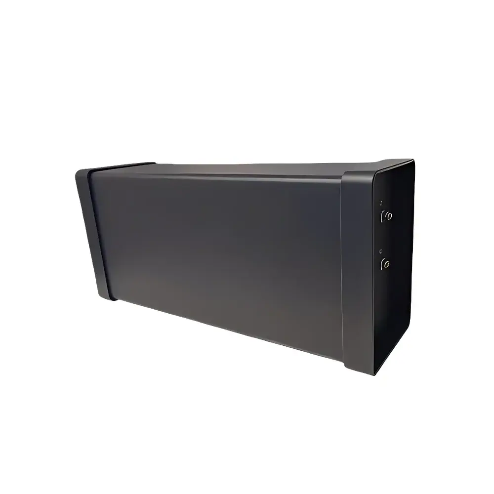
LBIC Laser-Induced Current Mapping System
| Origin | Japan |
|---|---|
| Manufacturer Type | Authorized Distributor |
| Origin Category | Imported |
| Model | LBIC |
| Price Range | USD 140,000 – 280,000 |
| Measurement Mode | AC-coupled photocurrent detection |
Overview
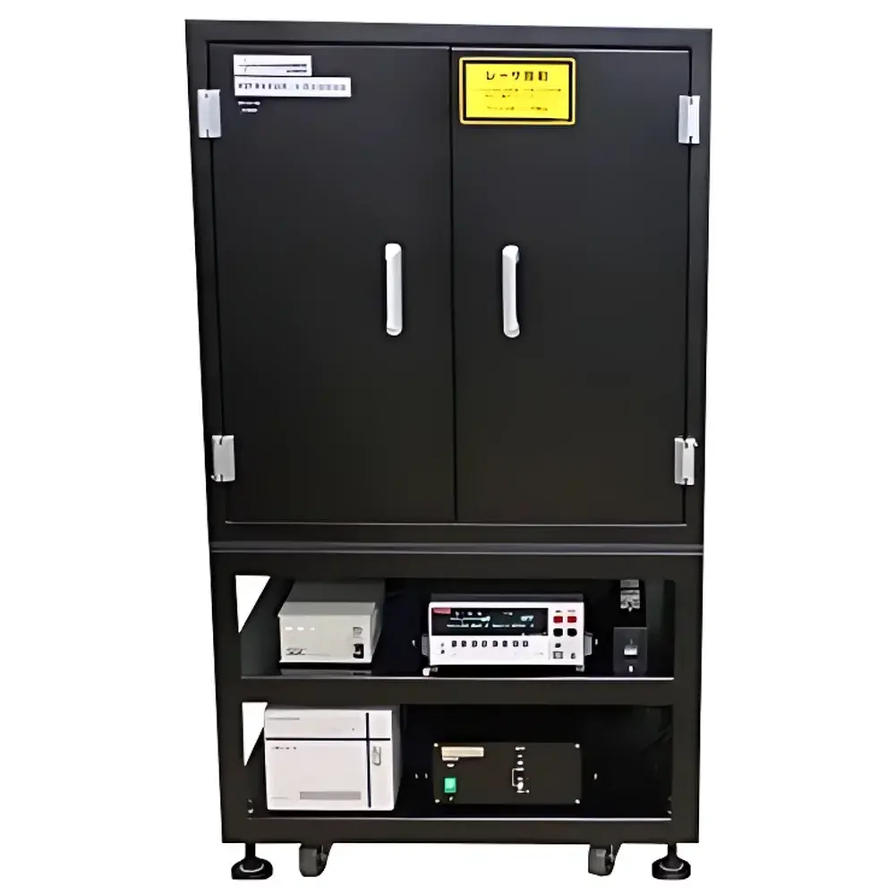
The LBIC Laser-Induced Current Mapping System is a precision optoelectronic characterization platform engineered for spatially resolved photocurrent analysis of photovoltaic (PV) devices. Based on the principle of laser-beam-induced current (LBIC) scanning, the system employs a focused monochromatic 532 nm green laser to locally excite charge carrier generation across the active area of solar cells, perovskite thin films, organic photovoltaics (OPVs), and other photoactive semiconductor structures. The resulting localized photocurrent is measured in real time using a high-sensitivity electrometer (Keithley Model 2401), enabling quantitative mapping of lateral variations in quantum efficiency, defect density, shunt resistance, and interfacial recombination. Designed for laboratory-based R&D and quality assurance workflows, the system delivers sub-100 µm spatial resolution and picoampere-level current sensitivity—critical for evaluating microscale heterogeneity in next-generation PV materials.
Key Features
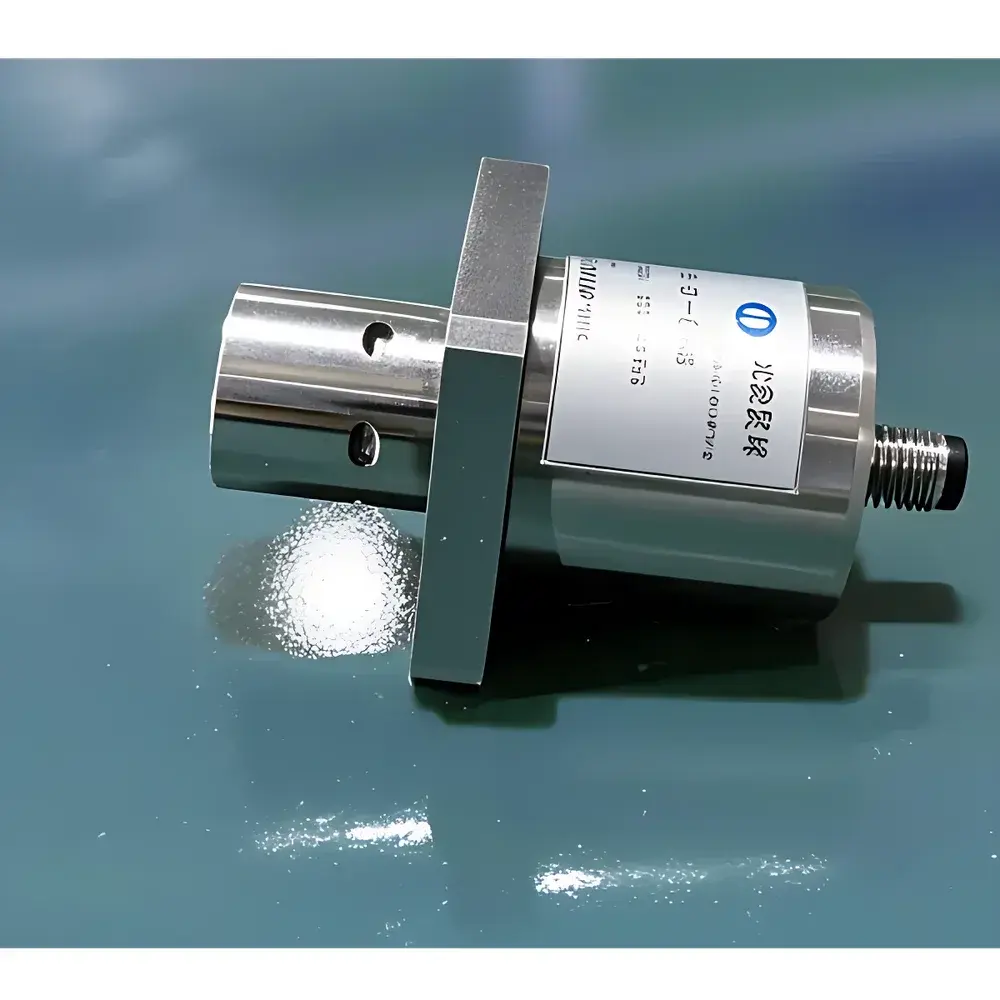
- Monochromatic 532 nm green laser source with stable output power ≤10 mW (±2% stability over 8 hours), optimized for silicon and perovskite bandgap excitation
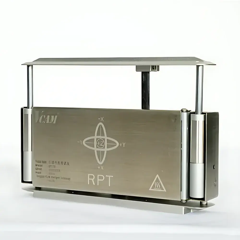
- High-precision XYZ motorized stage with ±30 mm travel range (50 × 50 mm effective scan area) and 1 µm step resolution
- Integrated CCD visual monitoring system with coaxial optical path for real-time sample alignment and laser spot positioning
- AC-coupled current measurement architecture minimizing DC drift and enabling robust signal-to-noise performance down to 10 pA
- Modular design supporting optional beam delivery configurations—including top-illumination, back-illumination, and edge-illumination modes—for comprehensive device architecture analysis
- Rugged mechanical housing and vibration-damped optical bench for stable operation in shared laboratory environments
Sample Compatibility & Compliance
The LBIC system accommodates rigid and flexible substrates up to 100 mm × 100 mm in footprint and ≤5 mm in thickness, including glass/ITO, FTO-coated quartz, metal foils, and polymer-based flexible PV stacks. Sample mounting uses non-contact vacuum chucking or adjustable mechanical clamps to avoid stress-induced artifacts. All electrical measurements conform to ASTM E1036–22 (Standard Test Methods for Electrical Performance of Nonconcentrator Terrestrial Photovoltaic Modules and Panels) and support traceable calibration against NIST-traceable reference cells. The system’s data acquisition firmware supports GLP-compliant audit trails, timestamped metadata logging, and user-access-controlled measurement protocols—fully compatible with ISO/IEC 17025 and FDA 21 CFR Part 11 requirements when integrated with validated laboratory information management systems (LIMS).
Software & Data Management
Control and analysis are performed via dedicated Windows-based software featuring intuitive GUI-driven scan setup, real-time current waveform visualization, and automated grid-based raster scanning. Raw current vs. position datasets are exported in HDF5 and CSV formats with embedded metadata (laser power, dwell time, filter settings, stage coordinates). Built-in post-processing tools include spatial derivative mapping (to identify grain boundaries and crack-induced shunts), normalized EQE estimation (when combined with calibrated spectral irradiance data), and statistical homogeneity metrics (e.g., coefficient of variation across ROI). Software architecture supports API integration (Python SDK) for custom automation, batch processing, and linkage to machine learning pipelines for defect classification.
Applications
- Quantitative mapping of local external quantum efficiency (EQE) and internal quantum efficiency (IQE) distributions in perovskite solar cells
- Identification and localization of shunting paths, pinholes, and interfacial delamination in multilayer thin-film devices
- Process development feedback for slot-die coating, vapor deposition, and thermal annealing steps
- Failure analysis of degraded modules through comparative LBIC imaging before/after accelerated aging (damp heat, thermal cycling)
- Correlation studies between LBIC maps and complementary techniques such as PL imaging, SEM-EBIC, and nanoscale Kelvin probe force microscopy (KPFM)
FAQ
What laser wavelength is used, and why is 532 nm selected?
The system uses a solid-state 532 nm green laser, chosen for its optimal absorption depth in common PV absorbers (e.g., ~1.2 µm in MAPbI₃, ~300 nm in c-Si), enabling selective excitation of the active layer without excessive substrate heating or carrier diffusion artifacts.
Can the system measure both forward and reverse bias conditions?
Yes—the Keithley 2401 source-measure unit supports four-quadrant operation, allowing simultaneous voltage bias application and photocurrent measurement under dark and illuminated conditions, essential for shunt resistance and diode ideality factor extraction.
Is spectral responsivity calibration included?
Calibration is not built-in but supported via external NIST-traceable reference photodiodes; users may perform absolute EQE calibration by integrating spectral irradiance data from a calibrated spectroradiometer.
How is laser spot size controlled and verified?
The Φ100 µm beam diameter is defined by a fixed aperture and confirmed via knife-edge profiling; optional beam expanders or focusing objectives can be installed for alternative spot sizes (e.g., 50 µm or 200 µm) upon request.
Does the software support automated reporting for QA/QC documentation?
Yes—customizable report templates generate PDF outputs with embedded maps, statistics, operator ID, timestamp, instrument configuration, and pass/fail thresholds aligned with internal quality control standards.