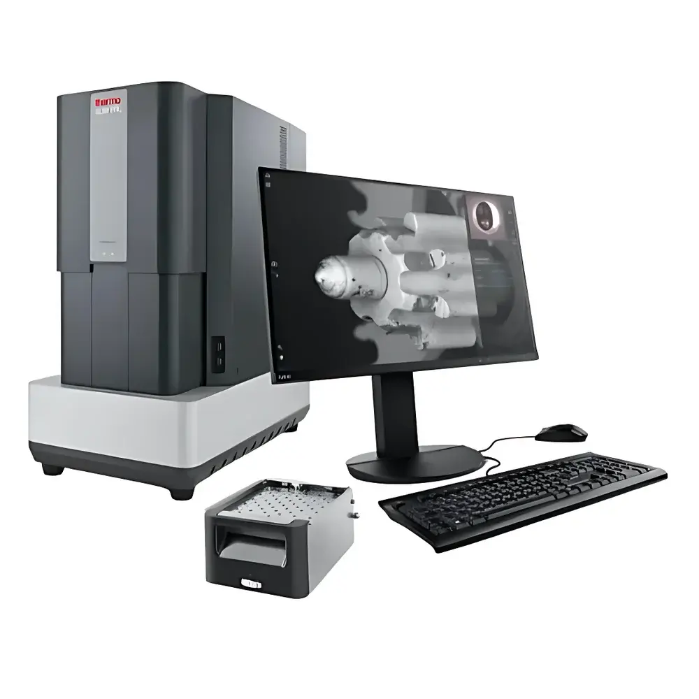
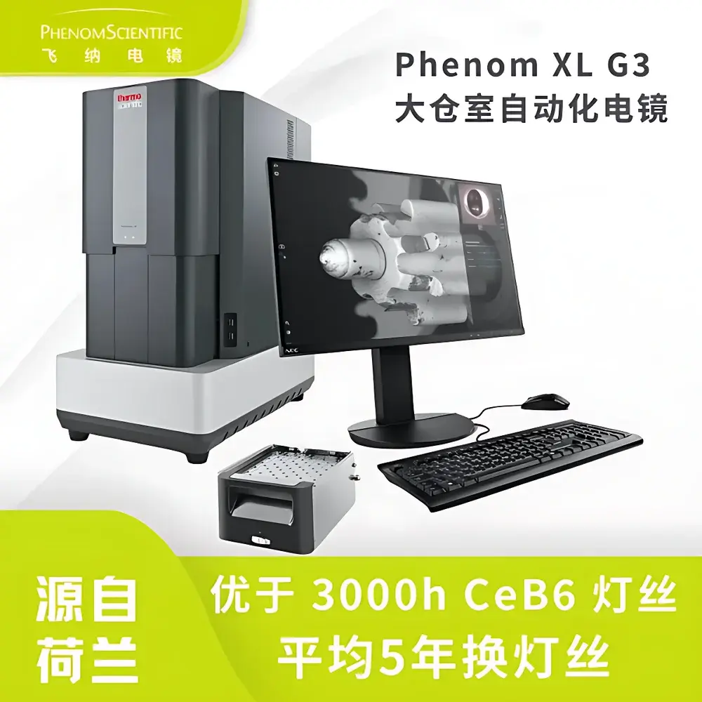
Phenom XL G3 Desktop Scanning Electron Microscope with Large Chamber
| Brand | Phenom (Thermo Scientific) |
|---|---|
| Origin | Netherlands |
| Instrument Type | Desktop SEM |
| Electron Source | CeB6 (Cerium Hexaboride) |
| Secondary Electron Resolution | <8 nm |
| Maximum Magnification | 200,000× |
| Accelerating Voltage Range | 4.8–20.5 kV |
| Backscattered Electron Resolution | <8 nm |
| Optional Detectors | EDS, Secondary Electron Detector |
Overview
The Phenom XL G3 Desktop Scanning Electron Microscope (SEM) is an industrial-grade, large-chamber SEM engineered for high-throughput, low-maintenance operation in non-traditional laboratory environments—including production floors, quality control labs on upper building levels, and even mobile or field-deployed settings. Leveraging over 80 years of electron optics heritage—from Philips’ foundational EM development (1939), through FEI’s commercialization of desktop SEM technology (2006), to Thermo Scientific’s current platform integration—the XL G3 embodies robust mechanical design, vacuum stability, and signal fidelity optimized for routine industrial analysis. Its core imaging mechanism relies on scanning a focused electron beam across the sample surface and detecting secondary electrons (SE) and backscattered electrons (BSE) to generate topographic and compositional contrast. The integrated CeB6 thermionic source delivers stable, high-brightness emission with exceptional longevity—rated for ≥3,000 hours—enabling continuous 7×24 operation without filament replacement for up to five years under typical QC usage.
Key Features
- Large chamber architecture accommodating samples up to 100 mm × 100 mm × 50 mm (W × D × H), eliminating frequent sample sectioning and enabling direct inspection of macro-scale components such as wafers, filters, fracture surfaces, and battery electrodes.
- Patented active vibration isolation system allows stable imaging without external anti-vibration tables—even on concrete floors, upper-story laboratories, or vehicle-mounted platforms.
- Optimized low-kV imaging capability (down to 2 kV) with enhanced BSE detector sensitivity and improved signal-to-noise ratio (S/N), enabling high-fidelity imaging of non-conductive, beam-sensitive, or uncoated specimens—including polymers, biological tissues, paper, and solar cell textures—without sputter coating.
- Automated workflow engine supporting full sequence control: auto-load, stage positioning, focus/stigmation, image acquisition, and report generation—all completed within ≤60 seconds per sample.
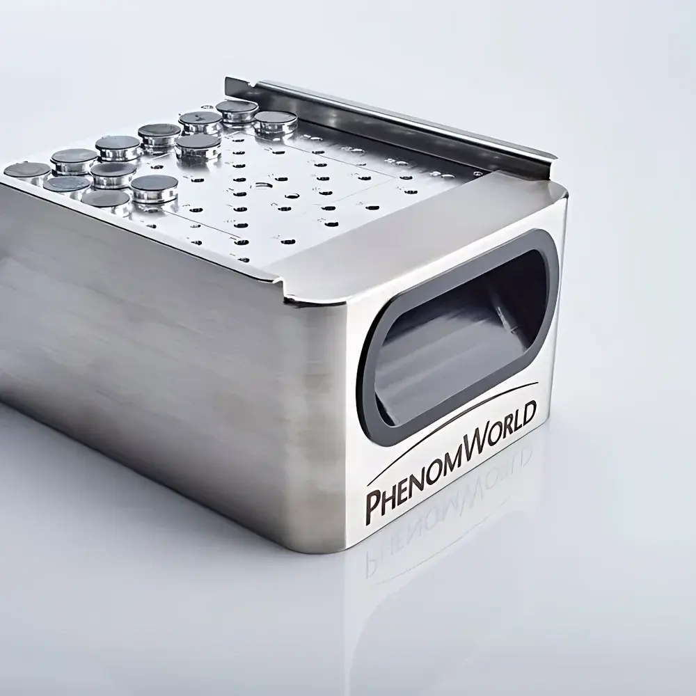
- Motorized 36-position sample carousel with programmable scripting interface (Python-based PPI) for unattended overnight batch analysis, compatible with LIMS and MES systems under Industry 4.0 frameworks.
- Integrated vacuum architecture with three selectable modes (low/medium/high vacuum) and sub-30-second pump-down time, minimizing downtime between analyses.
Sample Compatibility & Compliance
The XL G3 supports diverse material classes without mandatory conductive coating: ceramics, composites, metals, geological specimens, pharmaceutical powders, textiles, and electronic packaging materials. Its low-voltage SE/BSE imaging preserves surface integrity and mitigates charging artifacts in insulators. For regulated environments, the system supports audit-ready data handling: all image metadata (accelerating voltage, working distance, dwell time, detector gain) are embedded in TIFF headers; acquisition logs include timestamps, operator ID, and instrument configuration snapshots. While not certified to ISO/IEC 17025 out-of-the-box, the platform meets foundational requirements for GLP-compliant documentation when deployed with validated SOPs and controlled software versions. EDS integration complies with ASTM E1508 and ISO 16573 standards for quantitative elemental microanalysis.
Software & Data Management
Phenom’s native software suite provides unified control of imaging, spectroscopy, and analytics—no software switching required. ChemiSEM enables real-time elemental mapping by synchronously acquiring BSE and EDS spectra pixel-by-pixel, rendering color-coded phase distributions directly during acquisition. ChemiPhase performs statistical phase identification using multivariate clustering algorithms applied to EDS spectral libraries, outputting area-weighted phase fractions per region of interest. Phenom MAPS implements hierarchical tiling for seamless stitching of large-area scans (up to 100 mm²), embedding spectral data layers within the mosaic for post-acquisition re-analysis. ParticleMetric and FiberMetric modules automate ISO 13322-2–compliant particle sizing, shape classification (aspect ratio, circularity, convexity), and fiber length/diameter distribution reporting—with PDF/Excel export and customizable templates aligned with internal QA/QC protocols.
Applications
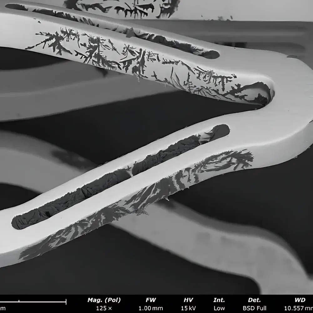
- Quality assurance of additive-manufactured metal parts: pore detection, grain boundary analysis, and inclusion characterization at ≤8 nm resolution.
- In-line inspection of lithium-ion battery cathodes/anodes: electrode homogeneity assessment, crack propagation tracking, and SEI layer morphology evaluation at 2–5 kV.
- Failure analysis of semiconductor packages: delamination mapping, solder joint void quantification, and contamination identification via EDS-guided navigation.
- Geological thin-section analysis: mineral phase discrimination in clays and carbonates using BSE contrast and ChemiPhase classification.
- Medical device surface evaluation: polymer scaffold porosity measurement, coating uniformity verification, and particulate residue detection on implants.
FAQ
Does the XL G3 require a dedicated SEM lab or special facility modifications?
No. Its built-in vibration damping, rapid vacuum cycling, and compact footprint enable installation in standard office or factory environments without floor reinforcement, RF shielding, or HVAC upgrades.
Can uncoated insulating samples be imaged reliably at high magnification?
Yes. The combination of CeB6 brightness, low-kV optimization (2–5 kV), and dual-detector signal processing enables stable, high-S/N imaging of ceramics, polymers, and biological specimens without sputter coating.
Is EDS data acquisition compliant with regulatory requirements for elemental quantification?
EDS analysis follows standard ZAF correction protocols and references NIST SRM standards. Full spectral data, acquisition parameters, and calibration logs are retained for traceability—supporting FDA 21 CFR Part 11 compliance when paired with appropriate IT governance controls.
What is the expected lifetime of the CeB6 source under continuous use?
Rated minimum lifetime is 3,000 operating hours. Under typical QC workflows (e.g., 8 hrs/day, 5 days/week), replacement intervals average 4–5 years, significantly reducing total cost of ownership versus tungsten or field-emission sources.
How does MAPS handle coordinate registration across stitched tiles?
MAPS uses motorized stage encoders and optical feedback to maintain sub-micron positional accuracy across tiles. Each tile retains absolute stage coordinates, enabling precise re-navigation to any pixel location in the composite map—even after system shutdown.


