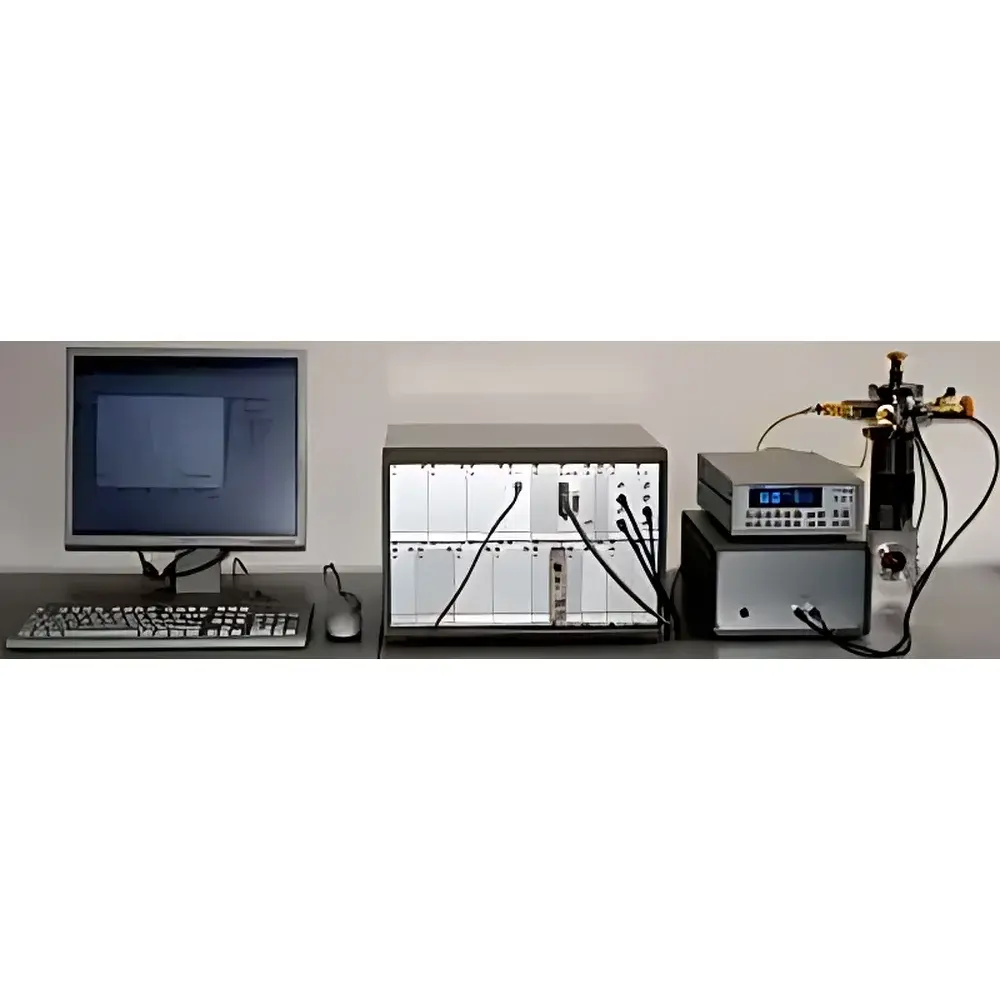
PhysTech FT1230 Deep Level Transient Spectroscopy System
| Brand | PhysTech |
|---|---|
| Origin | Germany |
| Model | FT 1230 |
| Measurement Principle | Capacitance- and Current-Based Transient Spectroscopy |
| Operating Modes | C-DLTS, CC-DLTS, I-DLTS, DD-DLTS, Zerbst-DLTS, O-DLTS, FET-Analysis, MOS-Analysis, ITS, PITS, TSC/TSCAP, DLOS |
| Software Features | Fourier-DLTS (F-DLTS), Laplace-DLTS, Multi-Exponential Transient Fitting, Isothermal Transient Signal Overlap, Temperature-Scan Signal Re-folding, User-Defined Correction Functions, Automatic Contact Check, Auto Capacitance Compensation |
| Cooling Compatibility | Liquid Nitrogen, Closed-Cycle Cryostats, Variable-Temperature Controllers |
| Sample Interface | Three-Terminal FET Configuration Support, Broad Capacitance & Doping Range |
| Compliance Framework | Designed for GLP/GMP-aligned semiconductor defect characterization workflows |
Overview
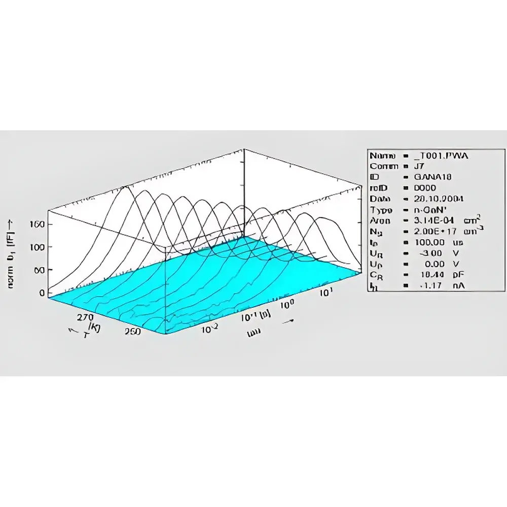
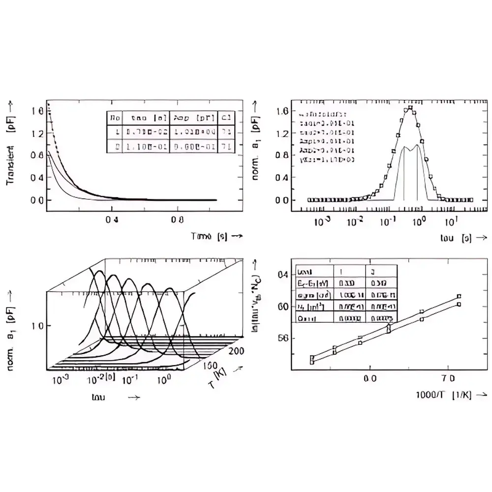
The PhysTech FT1230 Deep Level Transient Spectroscopy (DLTS) System is a high-precision, research-grade instrumentation platform engineered for quantitative identification and energy-resolved profiling of electrically active defects in semiconductor materials. Based on the fundamental principles of transient capacitance (C-t) and current (I-t) response analysis following controlled thermal or optical perturbation, the FT1230 implements standardized DLTS methodologies—including emission rate analysis, Arrhenius extraction, and trap activation energy determination—within a fully digitized, PC-controlled architecture. Introduced in 1990 as the world’s first all-digital DLTS system, the FT1230 leverages modern computational capabilities to execute real-time multi-exponential fitting, Laplace inversion, and Fourier-domain spectral decomposition—enabling sub-meV energy resolution and robust separation of overlapping trap signatures in complex junction structures.
Key Features
- Modular hardware architecture supporting seamless integration with cryogenic stages (LN₂ dewars, closed-cycle refrigerators) and precision temperature controllers (±0.1 K stability over 10–450 K range)
- Triple-terminal FET transient measurement capability for direct channel-current DLTS, enabling defect analysis in advanced field-effect device architectures
- Automated contact validation and real-time capacitance compensation—minimizing parasitic drift and improving baseline stability during long-duration scans
- Multi-mode operational flexibility: C-DLTS, CC-DLTS, I-DLTS, DD-DLTS, Zerbst-DLTS, O-DLTS (optically stimulated), ITS (isothermal transient spectroscopy), and PITS (photon-induced transient spectroscopy)
- Fourier-DLTS (F-DLTS) implementation with adjustable windowing functions, phase-sensitive detection, and user-definable correction algorithms for systematic artifact suppression
- Comprehensive defect parameter extraction suite: capture cross-section (σ), trap concentration (NT), thermal emission rate (en), activation energy (ET), and spatial distribution via C/V(T) and I/V(T) mapping
Sample Compatibility & Compliance
The FT1230 accommodates a broad spectrum of semiconductor substrates and device configurations—including Si, SiC, GaAs, InP, GaN, perovskite thin films, and MOS/MIS heterostructures—across capacitance ranges from 10 fF to >10 nF and doping densities spanning 1013–1018 cm−3. Its analog front-end design meets IEC 61000-4-3 immunity standards for laboratory electromagnetic environments. Data acquisition and processing comply with traceability requirements outlined in ISO/IEC 17025:2017 (Clause 7.7) and ASTM F1638-22 (“Standard Practice for DLTS Analysis of Semiconductor Defects”). Audit trails, electronic signatures, and version-controlled calibration logs are maintained in accordance with FDA 21 CFR Part 11 principles when configured with optional secure software modules.
Software & Data Management
The proprietary PhysTech DLTS Control & Analysis Suite provides a unified interface for instrument control, real-time visualization, and post-acquisition modeling. Raw transients are stored in HDF5 format with embedded metadata (temperature, bias, pulse parameters, hardware configuration). Mathematical engines support Laplace transform inversion (using the “filter diagonalization method”), multi-exponential least-squares fitting (Levenberg–Marquardt algorithm), and temperature-scan re-folding for enhanced signal-to-noise ratio. Export options include CSV, MATLAB .mat, and industry-standard SDF (Semiconductor Defect Format) for interoperability with TCAD tools such as Synopsys Sentaurus and Silvaco Atlas. All processing steps are logged with timestamps, operator ID, and parameter sets—ensuring full reproducibility and regulatory readiness.
Applications
- Identification and quantification of deep-level traps induced by ion implantation, epitaxial growth defects, or metal contamination in power devices
- Interface state density (Dit) profiling at Si/SiO₂ and wide-bandgap semiconductor/dielectric interfaces
- Reliability assessment of gate oxides under bias-temperature stress (BTS) and high-field stressing
- Defect engineering feedback for GaN HEMT buffer layer optimization and leakage path mitigation
- Correlation of DLTS spectra with minority-carrier lifetime (τeff) measurements from µ-PCD or QSSPC
- Validation of trap-assisted tunneling models in tunnel-FETs and resonant interband tunneling diodes
FAQ
What semiconductor materials are compatible with the FT1230?
The system supports elemental (Si, Ge), III–V (GaAs, InP), wide-bandgap (SiC, GaN, AlN), and emerging photovoltaic materials (perovskites, CZTS), provided standard Schottky or p–n junction fabrication protocols are followed.
Does the FT1230 support low-temperature operation below 80 K?
Yes—when coupled with a liquid helium cryostat or dilution refrigerator, the system maintains stable DLTS operation down to 4.2 K, enabling resolution of shallow traps (<50 meV) and quantum confinement effects.
Can raw DLTS data be exported for third-party analysis?
All transient waveforms, derivative spectra, and fitted parameters export in open formats (HDF5, CSV, MATLAB), with metadata conforming to the IEEE 1864-2021 standard for semiconductor metrology data exchange.
Is remote operation and monitoring supported?
The control software includes TCP/IP-based remote access functionality, allowing secure off-site experiment initiation, real-time progress tracking, and alarm-triggered notifications via configurable email/SNMP protocols.
How is calibration traceability maintained?
Capacitance and current channels are factory-calibrated against NIST-traceable reference standards; annual verification kits and documented procedures are supplied to support ISO/IEC 17025 internal audits.


