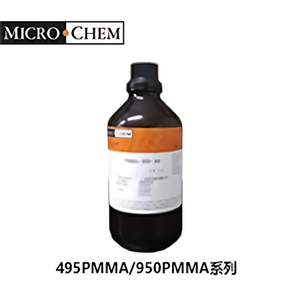
MicroChem PMMA Electron-Beam Positive Photoresist

| Brand | MicroChem Corp |
|---|---|
| Origin | Germany |
| Distributor Type | Authorized Distributor |
| Import Status | Imported |
| Model | PMMA |
| Pricing | Available Upon Request |
Ask about pricing, availability and specifications.
Overview
MicroChem PMMA Electron-Beam Positive Photoresist is a high-purity, solvent-based polymer resist system engineered for nanoscale lithographic patterning in advanced semiconductor R&D and prototyping environments. Based on poly(methyl methacrylate) (PMMA), this resist operates via chain scission upon exposure to high-energy electrons—enabling precise, high-resolution positive-tone development with sub-10 nm feature definition under optimized e-beam conditions. Unlike optical resists, PMMA exhibits negligible absorption at 10–100 keV electron energies, resulting in minimal forward scattering and superior resolution in direct-write electron beam lithography (EBL) systems. Its well-characterized dissolution kinetics, low outgassing rate, and thermal stability up to 180 °C make it suitable for demanding applications including gate stack fabrication, quantum device patterning, and MEMS/NEMS maskless prototyping.
Key Features
- High-resolution positive-tone resist optimized for 10–100 keV electron beam exposure
- Chain-scission mechanism ensures predictable contrast and high gamma (γ > 3.5) in standard developers (e.g., MIBK:IPA 1:3)
- Broad film thickness tunability—from 50 nm to >2 µm—via spin-coating at 1,000–6,000 rpm using standardized process parameters
- Excellent adhesion to silicon, SiO₂, SiNₓ, GaAs, InP, and metal substrates without requiring HMDS priming
- Low residual stress (< 50 MPa) and high thermal stability support post-litho annealing and lift-off compatibility
- Available in both homopolymer (PMMA) and copolymer (MMA-8.5%) formulations for dual-layer lift-off and profile-controlled patterning
Sample Compatibility & Compliance
PMMA resist demonstrates consistent performance across 100 mm, 150 mm, and 200 mm wafers, as well as non-planar substrates such as TEM grids and flexible polymer films. It is compatible with standard cleanroom solvents (acetone, IPA, PGMEA) and common etchants (CF₄/O₂ plasma, BCl₃/Cl₂, BOE). The formulation complies with ISO 14644-1 Class 5 cleanroom handling requirements and is manufactured under controlled ambient conditions to ensure ≤1 particle/µL (≥0.2 µm) contamination levels. While not classified as a GMP-grade material, PMMA meets ASTM F398 specifications for semiconductor photoresist purity and is routinely qualified for use in university cleanrooms, national labs (e.g., NIST, IMEC), and foundry pilot lines operating under GLP-aligned documentation practices.
Software & Data Management
MicroChem provides comprehensive process documentation—including spin-coating curves, bake profiles, exposure dose calibration tables (D₀, E₀), and developer concentration guidelines—for integration into automated lithography workflows. All technical data sheets are version-controlled and compliant with ISO/IEC 17025 documentation standards. For traceability in regulated environments, users may log exposure parameters (dose, dwell time, beam current) and processing steps in LIMS-compatible formats. While PMMA itself does not require software-driven dispensing, its compatibility with industry-standard tools—including Raith ELPHY Quantum, JEOL JBX-6300FS, and Zeiss Sigma VP—ensures seamless alignment with existing e-beam control platforms supporting ASCII-based pattern file import (GDSII, OASIS).
Applications
- Direct-write electron beam lithography for quantum dot arrays, superconducting qubit structures, and plasmonic metasurfaces
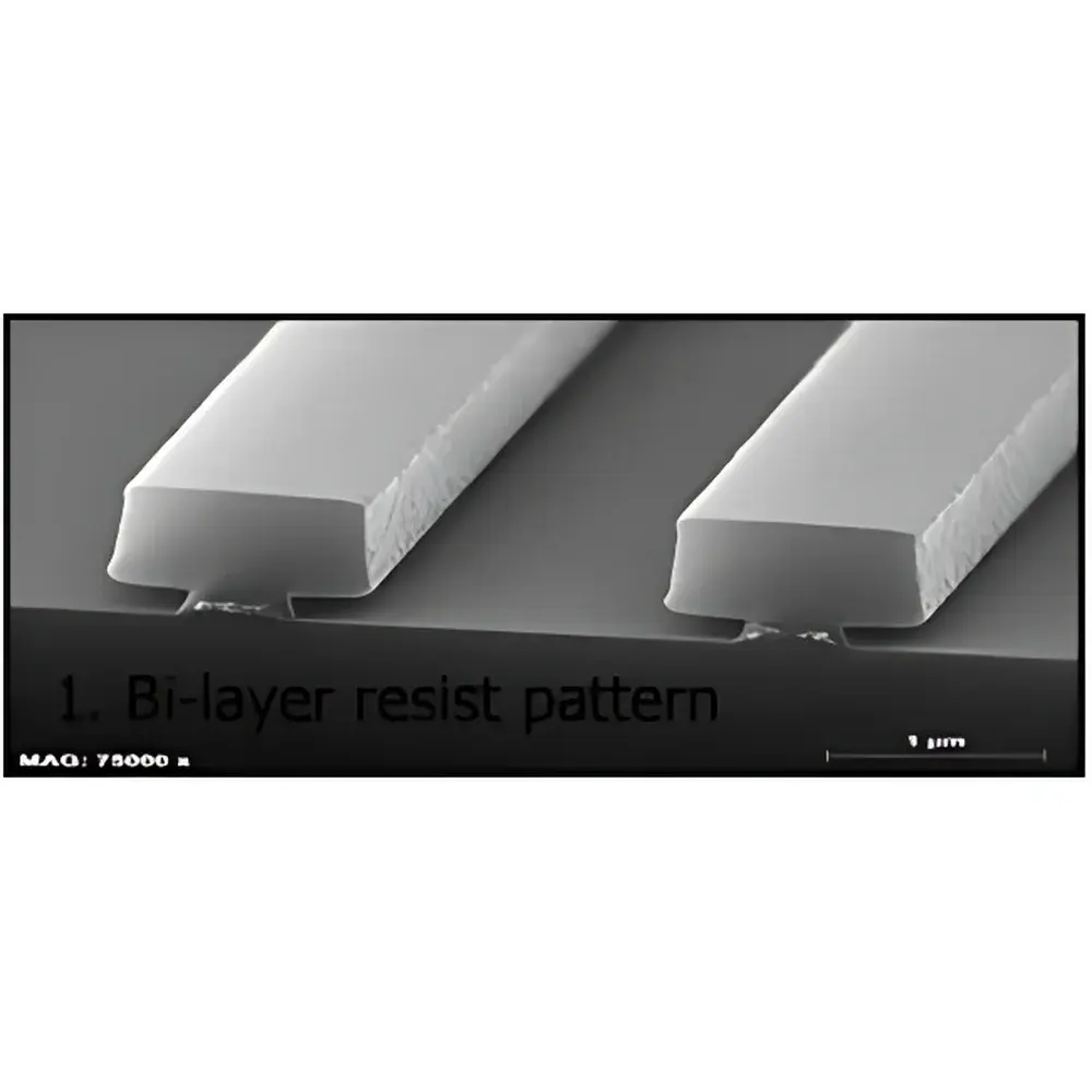
- Multi-layer lift-off processes using PMMA/MMA-8.5 bilayers to decouple critical dimension (CD) control from sidewall angle tuning
- Wafer thinning protection layers during back-grinding and dicing—leveraging PMMA’s mechanical toughness and chemical inertness
- Temporary bonding/debonding adhesive layers in TSV and 3D-IC stacking processes
- Hardmask precursor for high-aspect-ratio dry etching of Si, GaN, and AlN substrates
- X-ray lithography (synchrotron-based) where high radiation resistance and uniform cross-section are required
FAQ
What is the typical sensitivity range for PMMA under 100 keV electron beam exposure?
PMMA exhibits a dose sensitivity between 200–600 µC/cm² depending on molecular weight (e.g., MW = 950k vs. 2M), film thickness, and development chemistry.
Can PMMA be used in combination with deep UV or EUV lithography?
No—PMMA is not formulated for optical exposure; its absorption spectrum lacks sensitivity below 200 nm, making it unsuitable for DUV/EUV projection systems.
Is PMMA compatible with aqueous developers?
Yes—standard development uses organic solvents (e.g., methyl isobutyl ketone/isopropanol mixtures); aqueous bases like NaOH or TMAH are not recommended due to hydrolytic instability.
Does MicroChem provide lot-specific QC certificates?
Yes—each batch includes CoA documentation listing viscosity (cP), solids content (% w/w), residue on evaporation, and particulate count per ISO 14644-1 Annex B.
How should PMMA be stored to maintain shelf life?
Store unopened bottles at 4 °C in amber glass containers under nitrogen purge; shelf life is 12 months from manufacture date when stored per SDS guidelines.