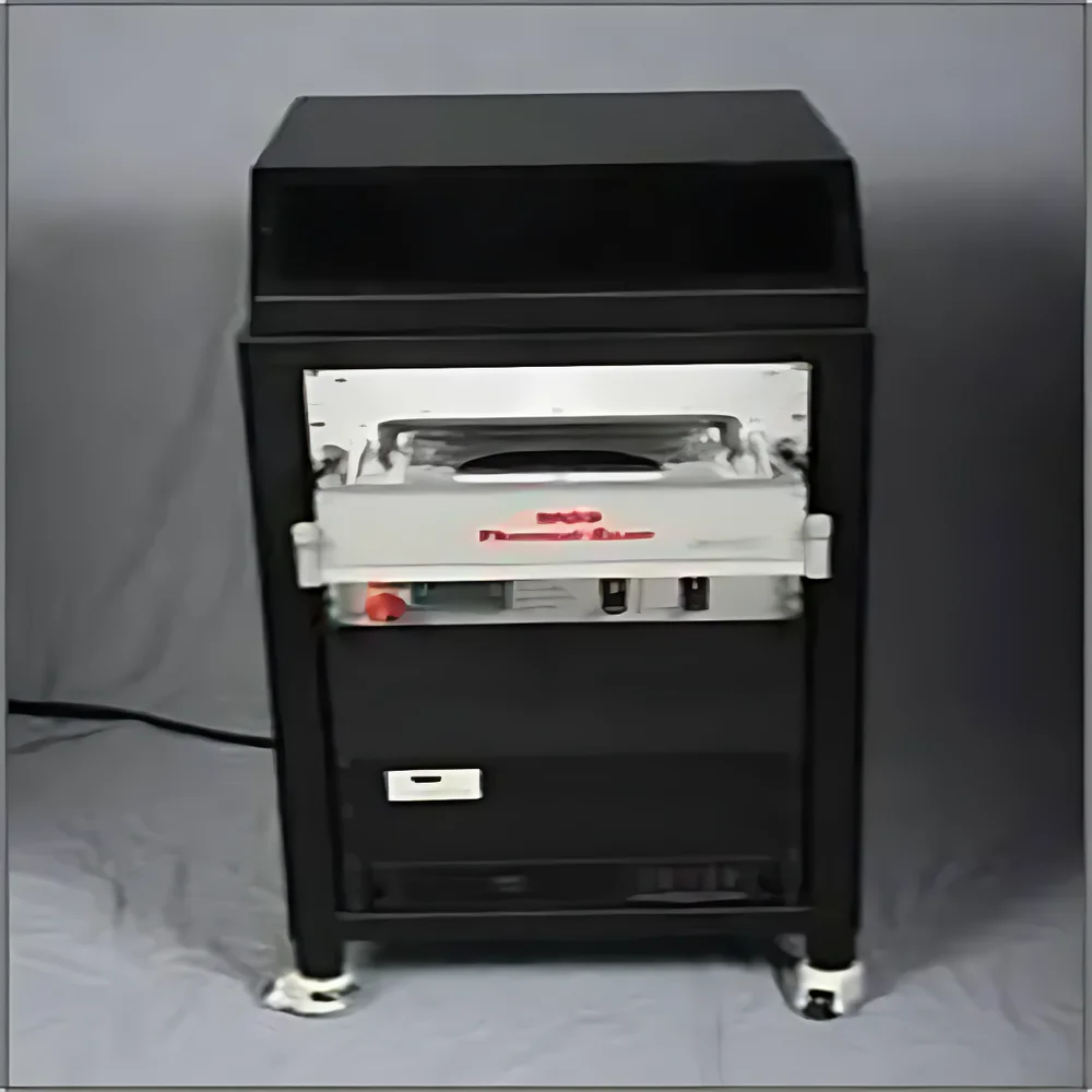
Microphase Thermal Scan Thin-Film Thermal Stress Measurement System

| Brand | Microphase |
|---|---|
| Origin | Japan |
| Model | Thermal Scan |
| Temperature Range | RT to 1000 °C (under vacuum or low-pressure gas ambient) |
| Curvature Resolution | 100 km |
| Curvature Repeatability | <2×10⁻⁵ m⁻¹ |
Ask about pricing, availability and specifications.
Overview
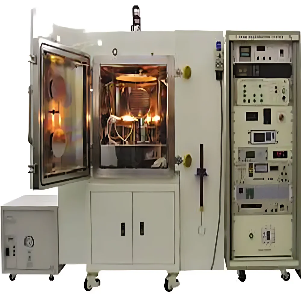
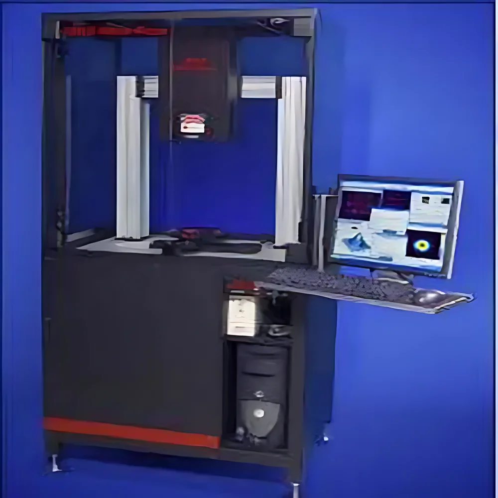
The Microphase Thermal Scan Thin-Film Thermal Stress Measurement System is a high-precision optical instrument engineered for in-situ, non-contact characterization of thermally induced mechanical response in thin-film structures. It operates on the Stoney equation principle, where curvature changes of a substrate—induced by thermal expansion mismatch between film and substrate—are optically measured via multi-beam interferometric deflection detection. This enables quantitative derivation of biaxial stress, stress gradient, and wafer-scale warpage as functions of temperature. Designed for research and process development labs in semiconductor, MEMS, photovoltaics, and advanced packaging industries, the system supports controlled thermal environments from ambient to 1000 °C under vacuum or regulated low-pressure inert/oxidizing atmospheres—ensuring relevance to real-world deposition, annealing, and post-processing conditions.
Key Features
- Patented Multi-Beam Optical Sensing (MOS) technology: A two-dimensional laser array enables simultaneous acquisition of curvature across multiple spatial points, delivering high spatial resolution and statistical robustness without mechanical scanning.
- Integrated thermal chamber with dual-mode environmental control: Supports both high-vacuum (<10⁻⁵ mbar) and low-pressure gas (N₂, Ar, O₂) operation, enabling studies under oxidation-sensitive or reducing conditions.
- Precision closed-loop temperature control: Achieves ±0.5 °C uniformity across 100 mm substrates at 1000 °C, verified by embedded thermocouple arrays and real-time PID feedback.
- Rapid thermal transients: Capable of heating rates up to 100 °C/min and active gas-quench cooling down to 100 °C/min, facilitating kinetic analysis of stress relaxation and phase transformation effects.
- Real-time dual-curve acquisition: Synchronized measurement of curvature vs. temperature and stress vs. temperature, with timestamped metadata for traceable thermal history correlation.
- Programmable optical scan architecture: Supports region-of-interest selection, linear multi-point profiling, and full-field 2D curvature mapping—configurable via intuitive scripting interface.
- Quantitative 2D stress imaging: Converts curvature maps into calibrated stress distributions (MPa), including principal stress orientation and gradient analysis for anisotropic films.
Sample Compatibility & Compliance
The Thermal Scan accommodates rigid planar substrates ranging from 25 mm to 150 mm in diameter—including silicon, sapphire, fused silica, quartz, and metal-coated wafers—with minimal thickness constraints (≥0.3 mm). It complies with ISO 9001 calibration traceability requirements and supports GLP/GMP-aligned documentation workflows. All thermal profiles and optical measurements are timestamped and logged with hardware-enforced audit trails, meeting foundational expectations for FDA 21 CFR Part 11–compatible data integrity when integrated with validated LIMS or ELN platforms. The system’s gas delivery manifold conforms to SEMI F57 standards for ultra-high-purity gas handling in microelectronics environments.
Software & Data Management
The proprietary ThermalScan Control Suite runs on Windows-based industrial PCs and provides deterministic real-time acquisition at 100 Hz per beam channel. Raw curvature data is stored in HDF5 format with embedded metadata (temperature setpoint, gas flow rate, vacuum level, timestamp, operator ID). Stress calculation modules implement ASTM F390-22–recommended curvature-to-stress conversion protocols, including corrections for substrate thickness variation and Poisson’s ratio uncertainty propagation. Export options include CSV, MATLAB .mat, and industry-standard DIAdem-compatible formats. Software validation documentation (IQ/OQ protocols) and source code review packages are available upon request for regulated environments.
Applications
- Thermal budget optimization of ALD, PVD, and CVD processes
- Interfacial stress evolution during rapid thermal annealing (RTA) of high-κ dielectrics and metal gate stacks
- Stress relaxation kinetics in amorphous SiNₓ and SiO₂ films under nitrogen ambient
- Residual stress mapping in heterogeneous thin-film solar cell architectures (e.g., CIGS on flexible substrates)
- Warpage prediction and mitigation in fan-out wafer-level packaging (FOWLP) substrates
- Qualification of low-stress passivation layers for MEMS resonators and RF filters
- Fundamental studies of stress-induced cracking, delamination onset, and viscoelastic transition temperatures
FAQ
What substrates can be measured?
Standard configurations support rigid planar wafers from 25 mm to 150 mm diameter and ≥0.3 mm thickness; custom chucks are available for non-standard geometries.
Is the system compatible with cleanroom Class 100 environments?
Yes—the optical head and chamber are designed for Class 100 compatibility; optional ISO Class 5 integration kits include ESD-safe enclosures and HEPA-filtered purge lines.
Can curvature data be exported for third-party finite element modeling (FEM)?
Yes—full-resolution curvature matrices (X, Y, Z) are exportable in ASCII grid format, directly importable into ANSYS Mechanical, COMSOL Multiphysics, and Synopsys Sentaurus.
Does the system meet ASTM or ISO standards for thin-film stress measurement?
It implements the physical principles defined in ASTM F390-22 and ISO 7500-1 for curvature-based stress evaluation; full compliance documentation is provided with each installation.
How is temperature uniformity verified during operation?
Pre-installation thermal mapping is performed using calibrated micro-thermocouples across the heater zone; users receive a certified uniformity report valid for 12 months.