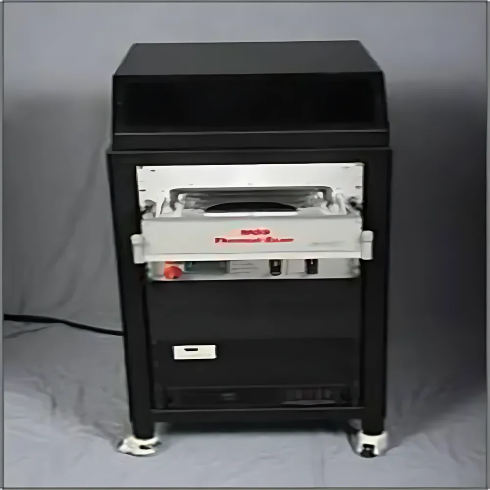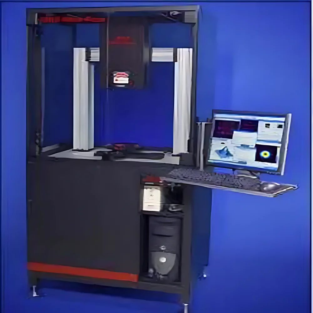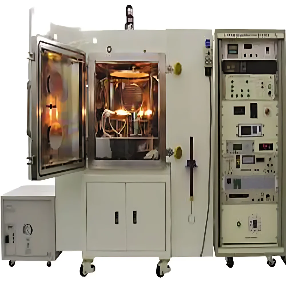
Microphase EBES Electron Beam Evaporation System

| Brand | Microphase |
|---|---|
| Origin | Japan |
| Model | EBES |
| Chamber Configuration | Cylindrical (φ500–1,500 mm × H800–1,500 mm) or Custom Rectangular |
| Electron Gun Options | Single, Dual, or Triple Source |
| Power Output | 6 / 10 / 15 / 20 kW |
| Beam Deflection Angle | 180° or 270° |
| Crucible Capacity | 7–40 cc (standard), up to 200 cc (UHV-compatible) |
| Substrate Size Range | 20–100 inches |
| Thickness Uniformity | < ±1.0% to ±5.0% |
| Optical Monitoring Range | 350–2000 nm (1 nm resolution) |
| Vacuum Performance | High Vacuum (1×10⁻⁷ Pa) to Ultra-High Vacuum (≤1×10⁻⁹ Pa) |
| Control System | PLC + Touchscreen PC with IC-5 / XTC / XTM Integration |
| Deposition Modes | Sequential or Concurrent Multi-Material Evaporation |
| Optional Modules | RF Bias, Ion Source, Mass Flow Controllers, Substrate Heating (up to 800 °C), Cryogenic Cooling, Plasma-Assisted Deposition |
Ask about pricing, availability and specifications.
Overview
The Microphase EBES Electron Beam Evaporation System is a precision-engineered thin-film deposition platform designed for high-reproducibility, high-purity material evaporation in semiconductor fabrication, optical coating, MEMS/NEMS development, and advanced research environments. Operating on the principle of electron beam heating—where a focused, high-energy electron beam impinges upon a refractory target material within a high-vacuum or ultra-high-vacuum environment—the system achieves localized thermal energy sufficient to vaporize materials with melting points exceeding 3,000 °C (e.g., Ta, W, Mo, SiO₂, Al₂O₃, ITO). Unlike resistive thermal evaporation, e-beam evaporation minimizes crucible contamination and enables stoichiometric transfer of complex oxides and alloys. The EBES architecture supports both single-source and multi-source configurations (dual or triple e-guns), permitting sequential or simultaneous co-evaporation of dissimilar materials—critical for graded-index optics, multilayer interference filters, and heterostructure device stacks.
Key Features
- Modular electron gun design with selectable power ratings (6 kW, 10 kW, 15 kW, or 20 kW) and beam deflection angles (180° or 270°) for optimized source-to-substrate geometry and shadowing control.
- Configurable crucible capacity: standard 25 cc (4- or 6-pocket) and 40 cc (4-pocket); extended options up to 200 cc for long-duration, high-throughput deposition—particularly suited for UHV-grade applications requiring minimal outgassing and thermal stability.
- Integrated real-time thickness monitoring via quartz crystal microbalance (QCM) and optical monitoring system (OMS): OMS covers 350–2000 nm spectral range with 1 nm wavelength resolution, enabling closed-loop control of optical multilayer stacks with sub-nanometer precision.
- Vacuum architecture scalable from high vacuum (HV, ≤1×10⁻⁷ Pa) to ultra-high vacuum (UHV, ≤1×10⁻⁹ Pa), supported by turbomolecular pumps, cryopumps, ion pumps, and calibrated ion gauges—ensuring low residual gas partial pressures critical for oxidation-sensitive films (e.g., MgF₂, LiF) and epitaxial-quality layers.
- PLC-based automation with industrial touchscreen PC interface, supporting full programmability of pump-down sequences, substrate rotation/heating/tilting, e-gun firing profiles, layer-by-layer thickness setpoints, and interlocked safety protocols.
- Expandable process capability: optional RF bias for ion-assisted densification, Kaufman-type ion source for pre-deposition surface cleaning or post-deposition ion bombardment, mass flow controllers for reactive gas introduction (O₂, N₂, Ar), and substrate temperature control up to 800 °C.
Sample Compatibility & Compliance
The EBES accommodates substrates ranging from 20-inch wafers to custom-sized optical flats (up to 100 inches), with planetary or linear rotation mechanisms ensuring uniform film distribution across large-area surfaces. Film uniformity is maintained at < ±1.0% (for small-area metrology-grade optics) to < ±5.0% (for production-scale semiconductor masks), validated per ISO 9001–certified calibration procedures. The system conforms to international vacuum safety standards (ISO 2746, EN 61000-6-4), electromagnetic compatibility (EMC) directives, and mechanical integrity requirements per CE Machinery Directive 2006/42/EC. For regulated environments—including ISO Class 5 cleanrooms and GMP-compliant pilot lines—the EBES supports audit-ready electronic logbooks, user access levels, and 21 CFR Part 11–compliant data integrity features when integrated with validated software packages (e.g., IC-5 with audit trail extension).
Software & Data Management
Control and data acquisition are managed through a deterministic real-time PLC backbone interfaced with a Windows-based HMI running proprietary or third-party deposition software (IC-5, XTC/XTM). All process parameters—including beam current/voltage, chamber pressure, substrate temperature, QCM frequency shift, OMS reflectance spectra, and shutter timing—are timestamped, logged at ≥10 Hz sampling rate, and exportable in CSV or HDF5 format. Software modules support recipe-driven multilayer synthesis, automatic thickness compensation based on real-time growth rate feedback, and cross-platform interoperability with factory automation systems (SECS/GEM, OPC UA). Data archiving complies with GLP/GMP documentation standards, including electronic signatures, version-controlled recipes, and immutable audit trails traceable to operator ID and system event logs.
Applications
- Semiconductor photomasks: Cr, MoSi, and TaN absorber layer deposition with sub-50 nm linewidth fidelity.
- Optical coatings: High-LIDT antireflection, high-reflectance dielectric stacks (TiO₂/SiO₂, Nb₂O₅/Ta₂O₅), and broadband polarizers for laser systems (193 nm to 10.6 µm).
- MEMS packaging: Hermetic AlN or SiO₂ capping layers with controlled stress and low hydrogen content.
- Quantum device fabrication: Superconducting Nb, NbN, and Al thin films under UHV conditions to preserve coherence length.
- Flexible electronics: Low-damage ITO and ZnO:Al deposition on PET/PEN substrates using low-energy e-beam rastering and substrate cooling.
- Research-grade MBE hybrid integration: Cluster tool configurations allow sequential e-beam evaporation and molecular beam epitaxy without air exposure.
FAQ
What vacuum level does the EBES achieve, and how is it verified?
The system achieves base pressures down to ≤1×10⁻⁹ Pa in UHV configuration, measured using dual ion gauges and cross-calibrated with residual gas analyzers (RGA). Pressure stability is monitored continuously during deposition and logged with every process record.
Can the EBES deposit multi-component alloys while maintaining stoichiometry?
Yes—via independent control of multiple e-guns with synchronized rate modulation and real-time OMS/QCM feedback, enabling precise compositional tuning (e.g., NiCr, TiAlN, or doped ZnO) without phase segregation.
Is remote operation and predictive maintenance supported?
Standard Ethernet/IP connectivity enables secure remote diagnostics, firmware updates, and performance analytics; optional vibration and temperature sensor arrays feed into predictive maintenance algorithms aligned with ISO 13374 standards.
How is contamination minimized between deposition runs?
UHV-grade stainless steel chamber construction, all-metal seals, in-situ plasma cleaning (with optional RF/ion source), and automated bake-out protocols reduce hydrocarbon and water partial pressures to <1×10⁻¹⁰ mbar prior to each run.
Does Microphase provide application engineering support for process transfer?
Yes—Microphase offers turnkey process qualification services, including film characterization (XRD, XPS, ellipsometry), deposition rate mapping, and DOE-based optimization for customer-specific materials and substrates.