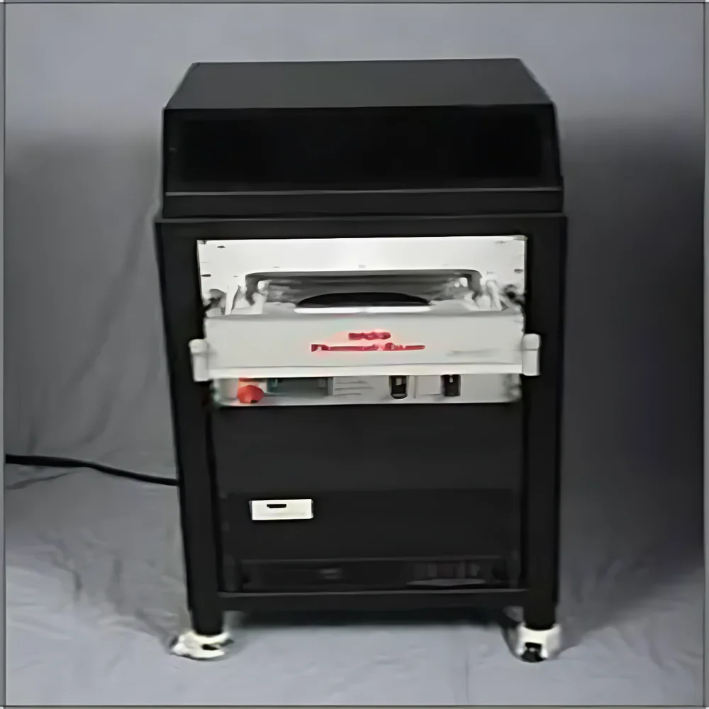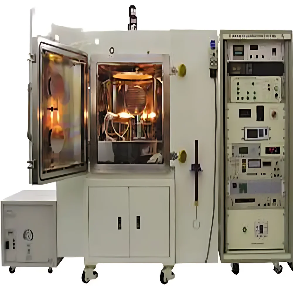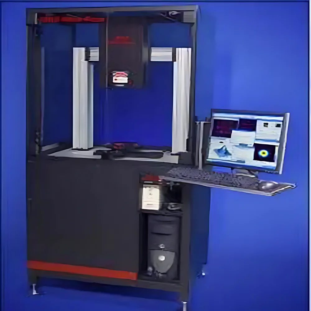
Microphase 12 Thin-Film Stress Measurement System

| Brand | Microphase |
|---|---|
| Origin | Japan |
| Model | 12 |
| Scan Range | 200 mm (X,Y) |
| Scan Speed | up to 20 mm/s (X,Y) |
| Scan Resolution | 2 µm |
| Mean Curvature Resolution | <2×10⁻⁵ m⁻¹ (1σ) |
| Temperature Range | −65 °C to 1000 °C |
| Measurement Principle | Non-contact Multi-Point Optical Shadow (MOS) Laser Interferometry |
Ask about pricing, availability and specifications.
Overview
The Microphase 12 Thin-Film Stress Measurement System is a high-precision, non-contact optical instrument engineered for quantitative in-plane stress and curvature characterization of thin films on rigid substrates. It operates on the principle of Multi-Point Optical Shadow (MOS) laser interferometry — a patented U.S. technology (US Patent No. 7,242,483 and related) that enables simultaneous, phase-synchronized detection of surface topography across an array of laser spots. Unlike single-beam profilometers or conventional wafer curvature scanners, the MOS architecture ensures all measurement points oscillate at identical frequency and phase, effectively decoupling mechanical vibration noise from curvature-derived stress calculations. This results in exceptional long-term stability and sub-microradian angular resolution, critical for detecting nanoscale stress gradients in epitaxial layers, dielectric stacks, or metallization films used in semiconductor fabrication, MEMS, and advanced packaging.
Key Features
- Programmable scanning modes: region-of-interest selection, multi-point linear profiling, and full-area raster scanning — configurable via intuitive GUI with script-based automation support.
- Real-time 2D curvature mapping: generates spatially resolved curvature (κx, κy, κxy) and Gaussian curvature maps with pixel-level quantification.
- Comprehensive stress analysis: calculates biaxial stress distribution (σxx, σyy, σxy) using Stoney’s equation and its generalized formulations, including thickness-dependent corrections and substrate anisotropy compensation.
- Integrated thermal control: compatible with industry-standard environmental chambers supporting temperature ramps from −65 °C to +1000 °C, enabling dynamic thermal stress profiling and activation energy extraction for stress relaxation mechanisms.
- Vibration-immune optical design: synchronized MOS beam array eliminates common-mode vibration artifacts without requiring active isolation tables — validated per ISO 20483-2 for laboratory-grade metrology environments.
Sample Compatibility & Compliance
The system accommodates wafers and planar substrates up to 200 mm × 200 mm, including silicon, sapphire, fused silica, quartz, glass, and ceramic carriers. Film thickness range spans from 10 µm (electroplated Cu), with no minimum optical absorption or reflectivity requirements due to robust shadow-edge detection. All measurements comply with ASTM F390-22 (Standard Test Method for Measuring Residual Stress in Thin Films by Curvature Technique) and are traceable to NIST-traceable length and angle standards. Data acquisition workflows support GLP/GMP audit trails and FDA 21 CFR Part 11–compliant electronic signatures when deployed with optional secure software licensing.
Software & Data Management
Control and analysis are performed using Microphase StressView™ v5.x — a Windows-based application featuring modular calibration wizards, batch processing queues, and export modules for HDF5, CSV, and TIFF formats. The software implements ISO/IEC 17025–aligned uncertainty propagation models, automatically reporting expanded uncertainty (k=2) for each curvature and stress value based on repeatability, thermal drift, and optical alignment tolerances. Raw interferogram time-series data are preserved alongside processed maps, enabling retrospective reanalysis and third-party validation. Optional API integration supports MATLAB, Python (via PyMicrophase), and LabVIEW for custom algorithm development and inline process monitoring interfaces.
Applications
- Process development and qualification of PVD, CVD, ALD, and electrochemical deposition tools — correlating film microstructure with residual stress evolution.
- Fundamental studies of stress relaxation kinetics during rapid thermal annealing (RTA) and furnace cycles.
- Reliability assessment of low-k dielectrics, high-κ gate oxides, and metal interconnects under thermo-mechanical cycling.
- Characterization of stress-induced buckling, delamination onset, and crack nucleation thresholds in flexible electronics and heterogeneous integration platforms.
- Calibration reference for finite element modeling (FEM) of multilayer stack behavior in IC packaging and optoelectronic devices.
FAQ
What physical principle does the Microphase 12 use to measure stress?
It employs non-contact Multi-Point Optical Shadow (MOS) laser interferometry to quantify substrate curvature changes induced by thin-film stress, then computes stress via Stoney’s equation and its tensor extensions.
Can it measure stress during film growth in vacuum?
Yes — the companion in-situ variant (Microphase 12-i) integrates directly into MBE, MOCVD, sputtering, PLD, and PECVD systems, maintaining full resolution under UHV conditions down to 10⁻⁸ Torr.
Is temperature calibration NIST-traceable?
All thermal stages include dual-point calibrated platinum RTDs with certificate of calibration traceable to NIST SRM 1750, and thermal uniformity is mapped per ASTM E220.
Does the system require periodic factory recalibration?
No — the MOS optical path is inherently drift-free; annual verification using certified step-height standards and curvature reference wafers satisfies ISO/IEC 17025 maintenance requirements.
How is data integrity ensured for regulated environments?
StressView™ supports role-based access control, electronic audit logs, and digital signature workflows compliant with FDA 21 CFR Part 11 and EU Annex 11 for pharmaceutical and medical device manufacturing QA/QC applications.