Microphase 11 In-Situ Thin-Film Stress Measurement System

| Brand | Microphase |
|---|---|
| Origin | Japan |
| Model | 11 |
| Scan Resolution | 2 µm |
| Mean Curvature Resolution | < 2×10⁻⁵ m⁻¹ (1-sigma, 50 km radius) |
| Mean Warp Measurement Repeatability | < 5×10⁻⁶ rad (1-sigma) |
| Mean Curvature Repeatability | < 2×10⁻⁵ m⁻¹ (1-sigma) |
Ask about pricing, availability and specifications.
Overview
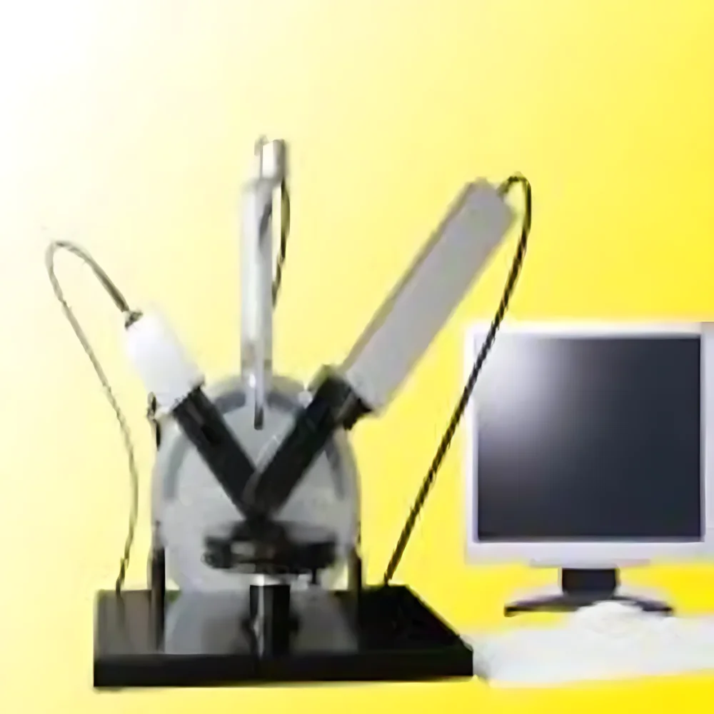
The Microphase 11 In-Situ Thin-Film Stress Measurement System is an optomechanical instrument engineered for real-time, non-contact quantification of mechanical stress evolution during thin-film deposition and post-processing. It operates on the principle of Multi-Point Optical Surface (MOS) interferometry—a patented U.S. technology that leverages spatially distributed laser spot arrays to detect nanoscale surface topography changes via curvature-induced beam deflection. By measuring localized surface slope gradients across a defined sample area, the system computes two-dimensional curvature maps, from which biaxial stress distributions are derived using Stoney’s equation and its generalized formulations. Designed for integration into high-vacuum and controlled-atmosphere environments, the Microphase 11 enables continuous monitoring during epitaxial growth (MBE, MOCVD), physical/chemical vapor deposition (sputtering, PECVD, PLD), and thermal annealing—without interrupting process integrity or requiring ex-situ handling.
Key Features
- Programmable scanning modes: region-of-interest selection, multi-point linear profiling, and full-area raster scanning—configurable via intuitive GUI with sub-micron positional fidelity.
- Real-time in-situ imaging: simultaneous acquisition of 2D curvature maps and quantitative stress distribution overlays at frame rates up to 10 Hz, supporting dynamic process correlation.
- Multi-parameter output: direct calculation and visualization of surface curvature (m⁻¹), radius of curvature (m), stress magnitude (MPa), stress gradient (MPa/mm), and global warp (radians).
- Vibration-immune architecture: synchronized laser array modulation ensures phase-coherent operation across all measurement points, suppressing low-frequency mechanical noise and enabling stable operation on standard optical tables without active isolation.
- Modular vacuum-compatible integration: flange-mounted optical head (CF-63 or ISO-KF40 options) with bakeable (<150 °C), UHV-rated (<1×10⁻⁹ mbar) housing; compatible with load-lock interfaces and RF-shielded chambers.
Sample Compatibility & Compliance
The Microphase 11 accommodates substrates ranging from 10 mm to 300 mm in diameter—including Si, GaAs, sapphire, fused silica, quartz, and flexible polymer foils—with no requirement for conductive coatings or surface preparation. Film thickness independence is achieved through differential curvature analysis, making it suitable for ultrathin layers (10 µm). The system complies with ISO 9001 calibration traceability protocols and supports GLP/GMP documentation workflows. Raw curvature data export formats (CSV, HDF5) are structured for audit-ready archiving, and software timestamps adhere to NIST-traceable UTC synchronization—enabling alignment with process log files for FDA 21 CFR Part 11–compliant environments where electronic records are subject to regulatory review.
Software & Data Management
Control and analysis are performed using Microphase Studio v4.x—a Windows-based application with dual-mode operation: standalone acquisition and API-integrated control (LabVIEW, Python SDK, MATLAB Instrument Control Toolbox). The software implements real-time background subtraction, thermal drift compensation algorithms, and user-definable stress transformation matrices for anisotropic substrates. All measurement sessions generate immutable metadata logs including environmental pressure, chamber temperature, time stamps, and operator ID. Exported datasets include calibrated curvature matrices, stress tensors, and statistical summaries (mean, std dev, min/max per ROI) compliant with ASTM F398-22 (Standard Practice for Measuring Thin-Film Stress Using Curvature Techniques). Audit trails record parameter changes, calibration events, and user actions—fully configurable for 21 CFR Part 11 electronic signature enforcement.
Applications
- In-situ monitoring of compressive/tensile stress transients during ALD cycle ramping and interfacial reaction kinetics.
- Quantifying thermal mismatch stress in III-V/Si heteroepitaxy and identifying critical thickness thresholds for dislocation nucleation.
- Correlating plasma-induced damage in PECVD SiNx films with curvature hysteresis during stepwise bias variation.
- Mapping stress gradients across wafer-scale OLED encapsulation layers to optimize barrier film uniformity.
- Validating finite-element models of MEMS release etch-induced warpage using experimental curvature boundary conditions.
FAQ
Does the Microphase 11 require substrate backside access or reference flat standards?
No. The system uses front-side only illumination and reflection detection; no backside polishing or reference wafer calibration is needed.
Can curvature data be exported for third-party finite element analysis (FEA)?
Yes. Full-resolution curvature matrices (X/Y/Z grids) are exportable in ASCII and HDF5 formats with SI-unit metadata, directly ingestible by ANSYS Mechanical, COMSOL Multiphysics, and ABAQUS.
Is the optical head compatible with ultra-high vacuum (UHV) systems operating below 10⁻¹⁰ mbar?
The standard CF-63 version is rated for 1×10⁻⁹ mbar; UHV variants with metal-sealed optics and low-outgassing materials are available under custom configuration.
How is thermal drift compensated during long-duration annealing measurements?
The system employs dual-wavelength referencing (635 nm + 785 nm) and real-time ambient temperature feedback from integrated PT100 sensors to decouple thermo-optic effects from mechanical curvature signals.
What is the minimum detectable stress change for a 500 nm SiO₂ film on a 100 mm Si wafer?
Based on Stoney’s equation and the specified curvature resolution, the theoretical lower limit is approximately ±0.8 MPa (1-sigma) under optimal signal-to-noise conditions.