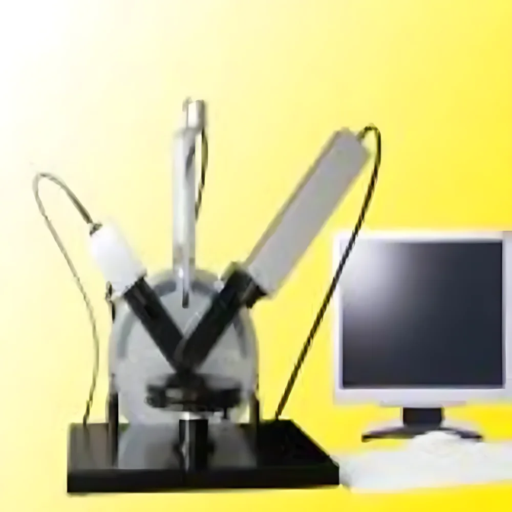
Microphase PHE Spectroscopic Ellipsometer

| Brand | Microphase |
|---|---|
| Origin | Japan |
| Model | PHE |
| Spectral Range | 250–1100 nm (optional deep-UV to IR extensions) |
| Incident Angle | 20°–90° |
| Spot Size | < 100 µm (configurable) |
| Measurement Speed | < 1 s per spectrum (typical) |
| Single Measurement Time | < 500 ms (at 1 nm resolution) |
| Sample Size Compatibility | Up to Ø200 mm wafers or 100 × 100 mm substrates |
| Spectral Resolution | ≤ 1 nm (standard), down to 0.2 nm (high-res option) |
| Thickness Accuracy | ±0.01 nm (for SiO₂ on Si reference) |
| Refractive Index Precision | ±0.0001 (n), ±0.0001 (k) |
| Psi/Delta Accuracy | ±0.01° / ±0.02° |
| Repeatability | < 0.005 nm RMS (thickness), < 0.00005 (n/k) over 24 h |
Ask about pricing, availability and specifications.
Overview
The Microphase PHE Spectroscopic Ellipsometer is a high-precision, research-grade optical metrology system engineered for non-destructive, contactless characterization of thin films and surface interfaces. Based on the fundamental principles of spectroscopic ellipsometry—measuring the change in polarization state (Ψ and Δ) of reflected light across a broad spectral range—the PHE delivers quantitative, model-independent determination of complex refractive index (n + ik), film thickness, interfacial roughness, and anisotropy in single-layer and multilayer structures. Its optical architecture integrates a high-stability broadband light source, precision rotating-compensator optics, and a thermoelectrically cooled CCD spectrometer, enabling robust operation under ambient laboratory conditions while maintaining sub-angstrom thickness resolution and ppm-level index stability. Designed for integration into cleanroom environments and R&D workflows, the PHE supports full spectral acquisition from 250 nm to 1100 nm—with optional deep-UV (190 nm) and near-IR (up to 2300 nm) configurations—making it suitable for advanced semiconductor process development, photonic device fabrication, and next-generation optoelectronic material studies.
Key Features
- Rotating-compensator design ensures high accuracy and long-term stability in Ψ/Δ measurement without moving parts in the detection path
- Variable incident angle control (20°–90°) with motorized goniometer and real-time angle calibration traceable to NIST standards
- Sub-micron spot size (<100 µm) with optional micro-spot module for localized analysis of patterned wafers and nanostructured surfaces
- Real-time spectral acquisition at up to 100 spectra per second, enabling dynamic in-situ monitoring of deposition and etch processes
- Modular optical head design allows field-upgradable spectral ranges—including deep-UV (190–400 nm) for high-k dielectrics and UV–Vis–NIR (250–2300 nm) for organic semiconductors and perovskites
- Integrated environmental enclosure with purge ports for nitrogen or dry-air operation, minimizing water vapor absorption in UV region
Sample Compatibility & Compliance
The PHE accommodates rigid and flexible substrates up to 200 mm in diameter or 100 × 100 mm square format, including silicon wafers, glass slides, quartz crystals, polymer foils, and metal-coated samples. It supports measurements on transparent, semi-transparent, and opaque substrates, as well as stacked heterostructures with up to 20 discrete layers. All hardware and software comply with ISO/IEC 17025 requirements for calibration traceability, and measurement uncertainty budgets are documented per JIS Z 8015 and ASTM E1938–22. For regulated environments, optional GLP/GMP-compliant audit trail logging, electronic signatures, and 21 CFR Part 11–ready configuration are available upon request.
Software & Data Management
The proprietary EllipSoft™ platform provides a unified interface for instrument control, optical modeling (using rigorous transfer-matrix formalism), and statistical data analysis. It includes built-in libraries of dispersion models (Cauchy, Tauc-Lorentz, Cody-Lorentz, B-spline), automated layer stack optimization with Levenberg-Marquardt and genetic algorithms, and batch processing for wafer maps. Raw Ψ/Δ spectra are stored in HDF5 format with embedded metadata (timestamp, environmental conditions, calibration ID). Export options include CSV, XML, and industry-standard SE data exchange formats (SE-XML v2.0). Remote access, API integration (Python/C++ SDK), and LIMS connectivity are supported via RESTful web services.
Applications
- Semiconductor process control: gate oxide thickness, high-k/metal gate stack composition, EUV resist characterization
- Photovoltaics: CIGS, perovskite, and organic PV layer uniformity, bandgap extraction, and degradation kinetics
- Optical coatings: anti-reflective, high-reflection, and dichroic filter design validation
- Biomedical thin films: protein adsorption kinetics on functionalized surfaces, hydrogel swelling behavior
- 2D materials: graphene monolayer coverage, h-BN thickness, and MoS₂ layer counting
- NIST-traceable reference measurements for national metrology institutes and inter-laboratory round-robin studies
FAQ
What spectral resolution is achievable with the standard PHE configuration?
Standard resolution is ≤1 nm FWHM across 250–1100 nm; high-resolution mode (≤0.2 nm) is available with optional grating and detector upgrade.
Can the PHE measure ultra-thin films (<0.5 nm) such as atomic layer deposited (ALD) seed layers?
Yes—sub-angstrom thickness sensitivity is routinely demonstrated on native oxides and ALD Al₂O₃ using multi-angle, multi-wavelength fitting with proper surface roughness parameterization.
Is vacuum operation supported?
The base system operates in air or purged environment; UHV-compatible variants (10⁻⁷ mbar) with differential pumping and load-lock integration are available as custom configurations.
How is calibration maintained between measurements?
Daily verification uses certified Si/SiO₂ reference wafers; factory calibration includes NIST-traceable angle encoder verification and spectral wavelength calibration with Hg/Ne emission lines.
Does the system support automated wafer mapping?
Yes—motorized XYZ stage with 0.1 µm repeatability enables full-wafer spectroscopic mapping (up to 1000 points) with programmable grid patterns and defect-triggered re-measurement logic.