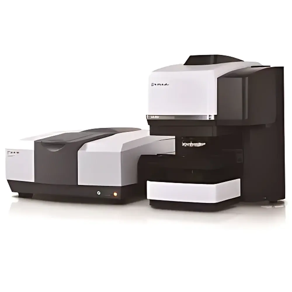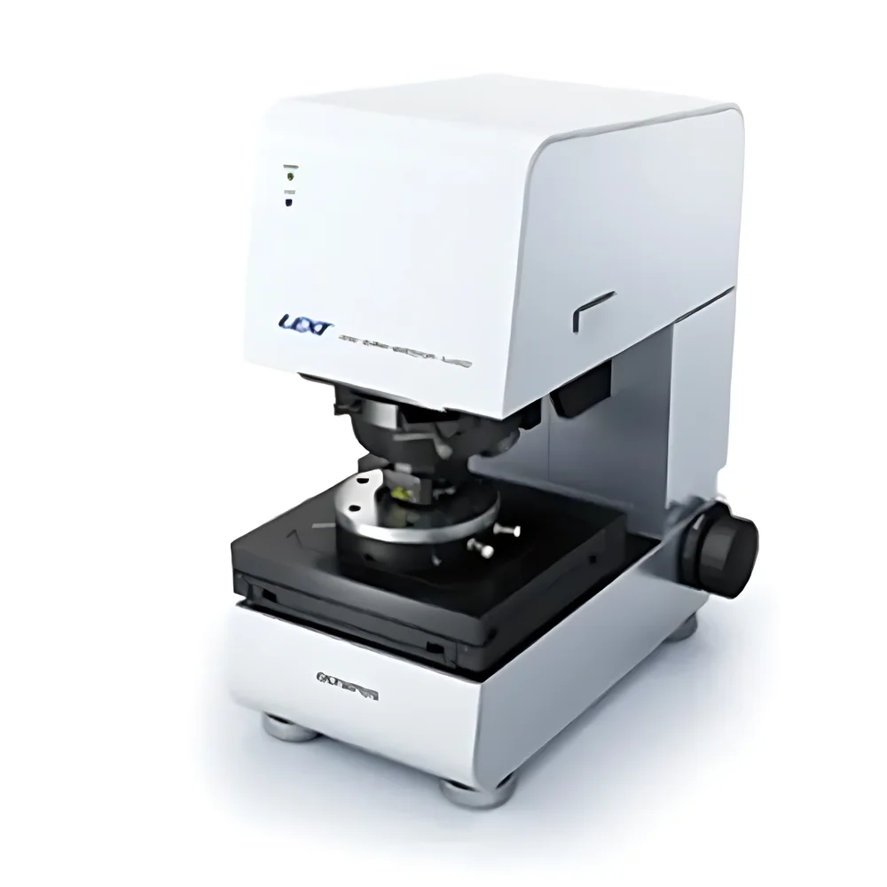
Shimadzu LEXT OLS4500 Laser Scanning Confocal Microscope

| Brand | Shimadzu |
|---|---|
| Origin | Japan |
| Model | LEXT OLS4500 |
| Type | Integrated Optical/Laser/SPM Hybrid Microscopy System |
| Laser Wavelength | 405 nm |
| Numerical Aperture (NA) | High-NA Objective Optimized for Confocal Imaging |
| Observation Modes | Brightfield (BF), Differential Interference Contrast (DIC), Simplified Polarization, HDR Imaging, Laser Confocal, Laser DIC, SPM Mode |
| Magnification Range | ~20× to 1,000,000× (continuous, multi-modal) |
| Z-Axis Resolution | Sub-nanometer (SPM mode) |
| XY Resolution | ≤120 nm (laser confocal, theoretical diffraction limit at 405 nm) |
| Scan Optical Zoom | Motorized, Continuous Variable |
| Software Platform | OLS4500 Dedicated Analysis Suite with Metrology & 3D Reconstruction Modules |
| Vibration Isolation | Compatible with Active/Passive Anti-Vibration Tables (optional integrated platform) |
Ask about pricing, availability and specifications.
Overview
The Shimadzu LEXT OLS4500 is an engineered hybrid microscopy platform that unifies three complementary imaging modalities—optical microscopy, laser scanning confocal microscopy (LSCM), and scanning probe microscopy (SPM)—within a single, co-registered optical path. Unlike conventional modular or add-on systems, the OLS4500 integrates these techniques at the hardware and software architecture level, enabling true in situ, multi-modal correlation without sample relocation or re-alignment. Its core measurement principle relies on confocal point-scanning optics using a 405 nm violet diode laser, high-numerical-aperture (NA) objective lenses, and precision piezo-driven Z-stage control to achieve sub-10 nm axial resolution in confocal mode. Combined with optical contrast mechanisms (BF, DIC, polarization, HDR), and contact/non-contact SPM functionality—including tip alignment jigs and navigable scan mapping—the system delivers traceable, quantitative 3D topography, surface roughness (Sa, Sq, Sz per ISO 25178), dimensional metrology (step height, width, angle), and nanoscale morphological characterization across length scales from millimeters to nanometers.
Key Features
- Multi-modal imaging architecture: Simultaneous optical, laser confocal, and SPM data acquisition on identical sample coordinates.
- 405 nm laser source with optimized high-NA objectives: Enables lateral resolution ≤120 nm and axial resolution <10 nm under standard environmental conditions.
- Motorized optical zoom and continuous magnification: Seamless transition from macro-scale survey (20×) to nanoscale detail (1,000,000× effective magnification via SPM).
- Dedicated contrast modes: Brightfield, differential interference contrast (DIC), simplified polarization, and high-dynamic-range (HDR) imaging—all accessible without hardware reconfiguration.
- Integrated SPM module with guided tip alignment: Eliminates manual laser spot adjustment; includes navigation-based region-of-interest (ROI) targeting using previously acquired overview images.
- Rigorous mechanical stability: Designed for compatibility with certified anti-vibration tables (e.g., active pneumatic or passive granite platforms) to ensure sub-nanometer Z-axis repeatability.
Sample Compatibility & Compliance
The LEXT OLS4500 accommodates rigid and semi-rigid solid samples up to 210 mm × 210 mm × 50 mm (W × D × H), including metallic alloys, ceramics, semiconductors, polished cross-sections, MEMS devices, and coated substrates. It supports non-conductive samples in optical and laser modes without metallization; conductive coating is required only for certain SPM electrical property measurements. The system complies with ISO 25178-601 (areal surface texture), ISO 21920-1 (linear surface texture), and ASTM E2923 (nanoscale dimensional measurement). Data acquisition and analysis workflows support audit-trail generation and user-access controls aligned with GLP and GMP documentation requirements. Exported measurement reports are compatible with FDA 21 CFR Part 11–compliant electronic record environments when deployed with validated IT infrastructure.
Software & Data Management
The proprietary OLS4500 Analysis Software provides unified control of all imaging modalities, real-time 3D reconstruction, automated roughness parameter calculation (per ISO 25178 series), and geometric feature extraction (e.g., line profiles, volume, curvature, grain analysis). Raw data is stored in vendor-neutral TIFF-based formats with embedded metadata (laser power, scan speed, NA, Z-step size, calibration timestamps). Batch processing, scriptable macros (via Python API), and export to CSV, STEP, or STL are supported. All user actions—including parameter changes, measurement annotations, and report generation—are logged with timestamped, immutable entries for full traceability. Software validation packages—including IQ/OQ documentation templates—are available for regulated laboratories.
Applications
- Failure analysis of microelectronic interconnects and solder joints
- Surface finish evaluation of orthopedic implants (Ra, Rz, Rsk per ISO 13565)
- Quantitative wear track depth and volume measurement in tribology studies
- MEMS device actuation characterization and stiction assessment
- Thin-film thickness and interface roughness analysis in PVD/CVD layers
- Particle morphology and agglomeration state assessment in pharmaceutical excipients
- Corrosion pit depth profiling and crack propagation mapping in aerospace alloys
FAQ
Does the LEXT OLS4500 require vacuum operation?
No. All optical, laser confocal, and SPM modes operate under ambient atmospheric conditions. Vacuum is not required or supported.
Can measurement data be exported for third-party statistical process control (SPC) software?
Yes. Dimensional and roughness parameters export directly to CSV or Excel-compatible formats, with column headers mapped to common SPC field definitions (e.g., “Feature_ID”, “Measured_Value”, “Tolerance_Upper”, “Timestamp”).
Is the system compliant with ISO/IEC 17025 calibration requirements?
The OLS4500 supports traceable calibration using NIST-traceable step-height standards and pitch standards. Shimadzu provides calibration certificates and uncertainty budgets per ISO/IEC 17025 Annex A.3 upon request.
What is the typical maintenance interval for the 405 nm laser module?
The solid-state 405 nm laser has a rated lifetime of ≥10,000 hours under nominal operating conditions. Preventive maintenance, including optical path alignment verification and objective lens cleaning, is recommended every 12 months or after 2,000 operational hours.
Can the system perform automated defect detection and classification?
While the base software does not include AI-based classification, the open API allows integration with external machine learning pipelines for custom defect segmentation and clustering using exported height maps and intensity data.