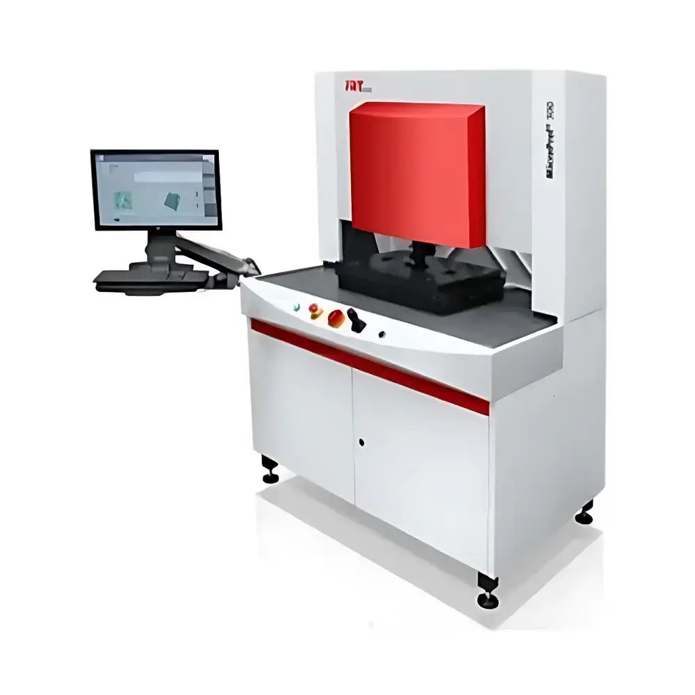
Camtek FRT MicroProf®100 Optical Surface Metrology System
| Brand | Camtek / FRT |
|---|---|
| Origin | Germany |
| Manufacturer Type | Authorized Distributor |
| Import Status | Imported |
| Model | MicroProf®100 |
| Detection Speed | Up to 50 million measurement points per wafer |
| 2D Lateral Resolution | 0.2 µm |
| 3D Vertical Height Accuracy | ±0.05 µm (measuring range: 2–100 µm) |
| Dual-Sided Measurement Capability | Yes (TTV/Bow/Warp/TIR/LTV) |
| Optical Principle | White-light Interferometry & Chromatic Confocal Sensing |
| Optional IR Sensor | Integrated for backside thickness monitoring of Si, GaAs, InP, SiC, GaN wafers |
| Compliance | SEMI Standard-compliant dual-probe architecture |
| Form Factor | Compact benchtop metrology platform |
Overview
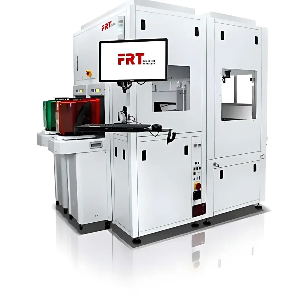
The Camtek FRT MicroProf®100 Optical Surface Metrology System is a high-precision, non-contact surface characterization instrument engineered for semiconductor process control and advanced packaging applications. It employs white-light interferometry and chromatic confocal sensing principles to deliver traceable, repeatable 3D topography, film thickness, and geometric parameter measurements—without physical contact or sample preparation. Designed specifically for front-end and back-end semiconductor manufacturing, the system supports full-wafer metrology on silicon, compound semiconductors (GaAs, InP, SiC, GaN), and transparent or opaque substrates. Its dual-probe configuration—featuring synchronized top and bottom optical heads—enables simultaneous acquisition of upper and lower surface profiles, enabling direct calculation of total thickness variation (TTV), bow, warp, total indicator reading (TIR), local thickness variation (LTV), and parallelism. The integrated infrared (IR) sensor option extends capability to monitor backside grinding processes by penetrating bulk semiconductor materials, providing real-time thickness feedback during wafer thinning.
Key Features
- Non-destructive, non-contact 3D surface metrology with sub-nanometer vertical resolution and 0.2 µm lateral resolution
- Dual-sided measurement architecture compliant with SEMI standards for TTV, bow, and warp quantification in a single scan
- Modular multi-sensor platform supporting white-light interferometry, chromatic confocal, and optional IR transmission sensing
- High-throughput acquisition: up to 50 million measurement points per 300 mm wafer in under 90 seconds
- Benchtop form factor with minimal footprint—ideal for cleanroom integration and R&D lab deployment
- SurfaceSens™ optical engine enabling seamless switching between areal, line, point, and layer-thickness measurement modes
- Field-upgradable TTV option for retrofitted dual-surface analysis without hardware replacement
Sample Compatibility & Compliance
The MicroProf®100 accommodates standard semiconductor wafers (100 mm to 300 mm), diced dies, MEMS devices, and compound semiconductor substrates—including both opaque (Si, SiC) and transparent (glass, sapphire, quartz) materials. It meets critical industry requirements for geometric metrology: ASTM E1390 (Standard Test Method for Measuring Thickness of Transparent Films), ISO 25178 (Geometrical Product Specifications – Surface Texture), and SEMI MF-1530 (Specification for Total Thickness Variation Measurement). For regulated environments, the system supports audit-ready data logging with time-stamped metadata, user access controls, and optional 21 CFR Part 11–compliant electronic signatures when paired with FRT’s certified software package.
Software & Data Management
Controlled via FRT’s proprietary WinWerth® software, the MicroProf®100 provides intuitive workflow configuration for manual or fully automated measurement sequences. All measurement tasks—including profile extraction, roughness analysis (Sa, Sq, Sz), step height quantification, film thickness modeling (for transparent layers), and geometric parameter reporting—are scriptable and repeatable. Raw data is stored in vendor-neutral formats (e.g., .xyz, .csv, .tif) and supports batch processing across multiple wafers. Traceability is ensured through embedded calibration logs, environmental sensor records (temperature/humidity), and operator-auditable change history. Integration with factory MES/SPC systems is enabled via SECS/GEM protocol support and OPC UA interface.
Applications
- Front-end process control: post-CMP thickness uniformity, etch depth verification, and lithographic resist profile analysis
- Back-end wafer-level packaging: bump height/volume metrology, redistribution layer (RDL) topography, and under-bump metallization (UBM) inspection
- Compound semiconductor manufacturing: epitaxial layer thickness mapping on GaN-on-Si or InP substrates
- MEMS device characterization: cavity depth, membrane flatness, and release etch uniformity assessment
- Advanced substrate qualification: TTV/bow/warp screening prior to bonding or lithography steps
- Research & development: quantitative surface evolution studies during thermal cycling, annealing, or stress testing
FAQ
Does the MicroProf®100 support automated wafer handling?
Yes—when integrated with third-party robotic load ports and cassette handlers, the system supports unattended operation for up to 25 wafers per run.
Can it measure transparent thin films on opaque substrates?
Yes—using spectral reflectance analysis within the white-light interferometry mode, it quantifies film thickness from 1 nm to 10 µm with layer-stack modeling capability.
Is calibration traceable to national standards?
All factory calibrations are NIST-traceable; on-site recalibration kits and accredited service contracts are available globally.
What environmental conditions are required for optimal performance?
Recommended operating range: 20–24 °C ±0.5 °C, humidity 40–60% RH, vibration isolation class ISO 22476-1 Class B.
How does the IR sensor function during backgrinding monitoring?
The integrated near-infrared (1310 nm) probe transmits through Si and GaAs substrates up to 1 mm thick, enabling real-time thickness tracking from the device side without flipping the wafer.


