
Scanning Electron Microscope
Filter
Showing 1–30 of 153 results
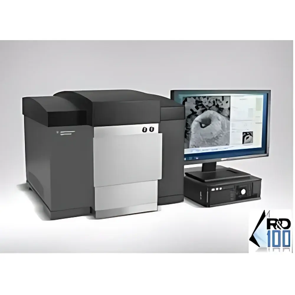
| Origin | USA |
|---|---|
| Manufacturer Type | Authorized Distributor |
| Origin Category | Imported |
| Model | 8500 |
| Price Range | USD 135,000 – 205,000 (FOB) |
| Electron Gun Type | Cold Field-Emission (CFE) |
| Secondary Electron Imaging Resolution | 10 nm @ 1 kV |
| Magnification Range | 250× – 800,000× |
| Accelerating Voltage | 0.5 – 2.0 kV |
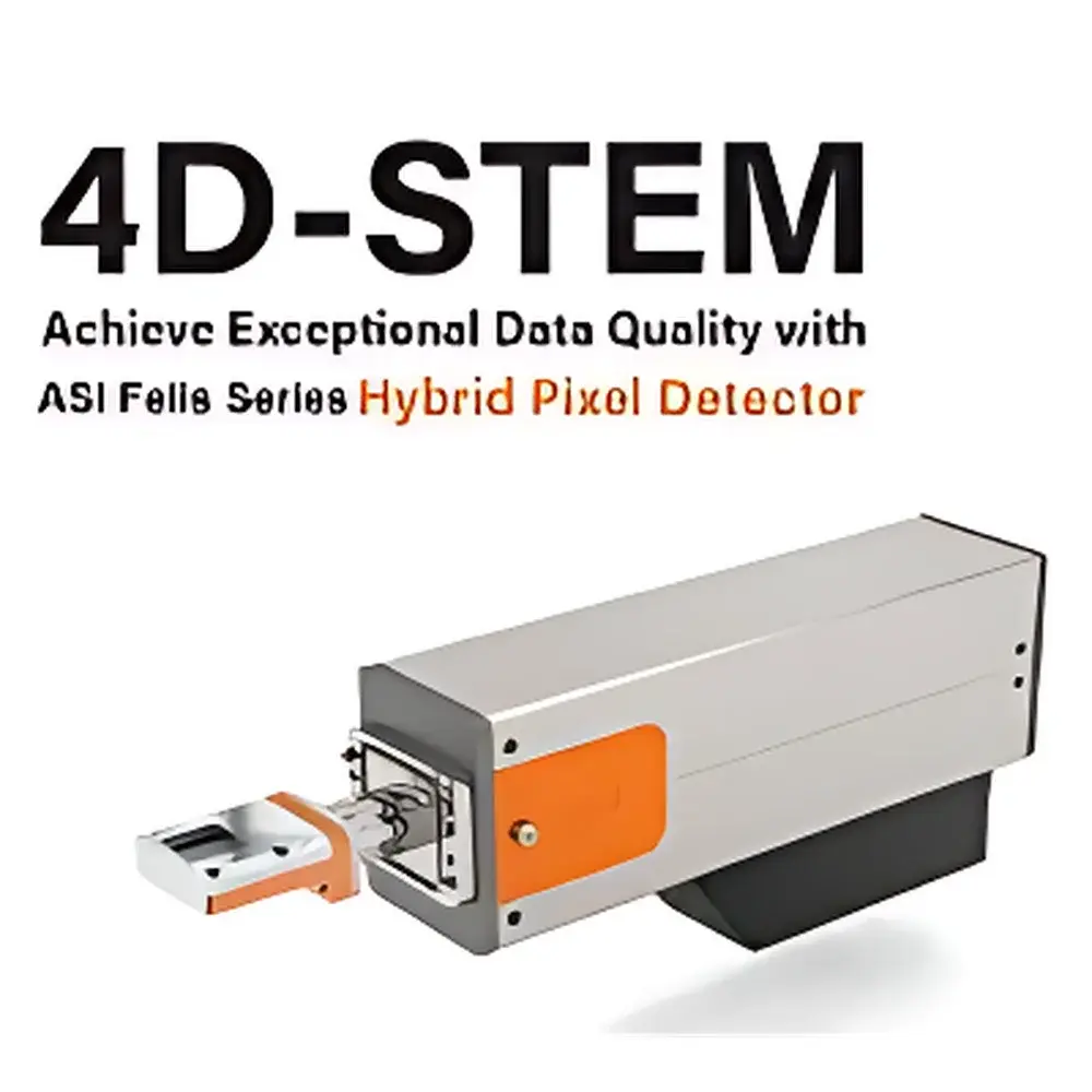
| Brand | Amsterdam Scientific Instruments (ASI) |
|---|---|
| Origin | Netherlands |
| Model | Felis T3 |
| Acceleration Voltage Range | 0.5–30 kV |
| Sample Stage | 5-position 3 mm TEM grid holder |
| Detector Type | Hybrid pixel detector with nanosecond timestamping capability |
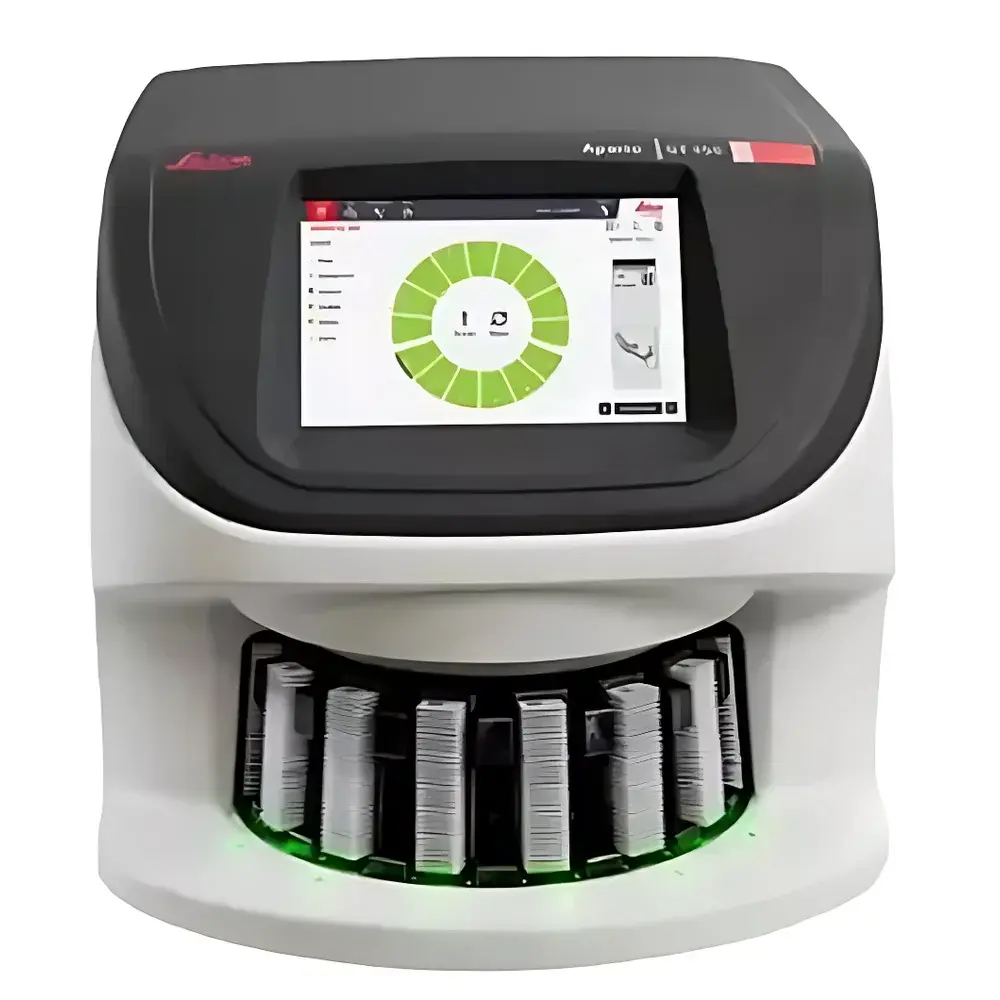
| Brand | Leica |
|---|---|
| Origin | Germany |
| Manufacturer Type | Authorized Distributor |
| Import Status | Imported |
| Model | Aperio GT450 |
| Electron Source | Cerium Hexaboride (CeB₆) |
| Scan Speed | 32 s per 15 mm × 15 mm area at 40× |
| Throughput | 81 slides/hour |
| Color Calibration | ICC-compliant medical-grade color profile (DICOM GSDF & sRGB aligned) |
| Optical System | Custom Leica 40× apochromatic objective with real-time autofocus |
| Intended Use | For Research Use Only (RUO) |
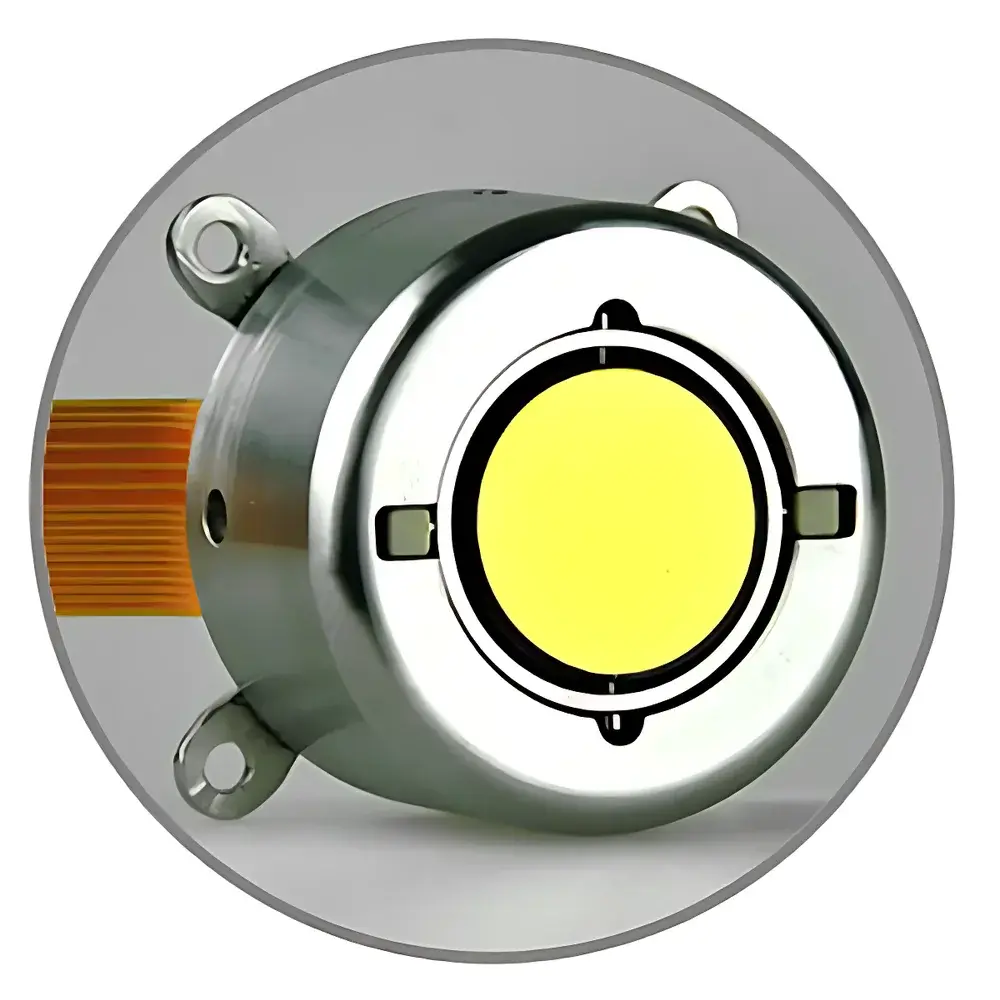
| Brand | Auniontech |
|---|---|
| Model | W |
| Actuator Type | 4-Quadrant (2-axis, bi-directional) |
| Mechanical Tilt Angle (DC) | ±25° (X & Y axes) |
| Mirror Diameter | 15 mm |
| Center of Rotation to Mirror Surface | 1.3 mm |
| External Diameter | 30 mm |
| Zero Drift | ≤25 µrad/°C |
| Closed-Loop Resolution | <5 µrad |
| Repeatability (RMS, typical) | 30–100 µrad |
| Full-Scale Bandwidth (Sine, ±25°) | 20 Hz |
| Small-Signal Bandwidth | 350 Hz |
| Large-Angle Step Response (20° step) | 7.5 ms |
| Small-Angle Step Response (0.1° step) | 1.4 ms |
| Instrument Form Factor | Benchtop |
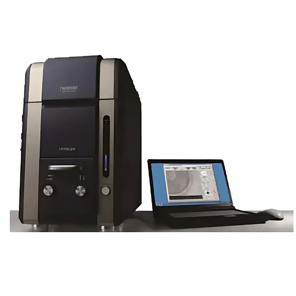
| Brand | BM |
|---|---|
| Origin | Shanghai, China |
| Model | TM3030 |
| Instrument Type | Desktop SEM |
| Electron Source | Pre-aligned Tungsten Filament |
| Accelerating Voltages | 5 kV, 15 kV |
| Magnification Range | 15× to 30,000× (with digital zoom: 2×, 4×) |
| Maximum Sample Diameter | 70 mm |
| Sample Stage Travel | X: ±17.5 mm, Y: ±17.5 mm |
| Detector System | High-sensitivity 4-segment semiconductor backscattered electron (BSE) detector |
| Vacuum System | Turbo-molecular pump (30 L/s), diaphragm pump (1 m³/h), ultimate vacuum ≤1.5×10⁻⁵ Pa, variable pressure mode (6–270 Pa, 22 steps) |
| Control Interface | Two USB 2.0 ports, Ethernet port |
| Operating System | Microsoft Windows® 7 or later |
| Display | 15.4-inch LCD (1280×800 resolution) |
| Auto-functions | Auto filament saturation, auto beam alignment, auto stigmation, auto focus, auto brightness/contrast, overcurrent protection, leakage circuit breaker |
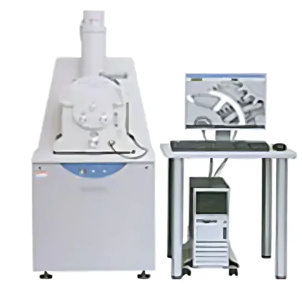
| Brand | BM |
|---|---|
| Origin | Shanghai, China |
| Model | U1510 |
| Instrument Type | Floor-standing SEM |
| Electron Source | Tungsten Filament |
| Vacuum Modes | High Vacuum & Variable Pressure (6–270 Pa) |
| Secondary Electron Resolution | 3.0 nm @ 30 kV (High Vacuum) |
| Backscattered Electron Resolution | 4.0 nm @ 30 kV (6 Pa, Low Vacuum) |
| Magnification Range | 5× to 300,000× |
| Accelerating Voltage | 0.3–30 kV |
| Max Sample Diameter | 153 mm |
| Stage Travel | X 0–80 mm, Y 0–40 mm, Z 5–50 mm, T –20° to +90°, R 360° |
| Standard Detectors | Everhart-Thornley-type Secondary Electron Detector (SED), High-Sensitivity Semiconductor Backscattered Electron Detector (BSE) |
| Vacuum System | Single Turbo-Molecular Pump + Rotary Mechanical Pump |
| Safety Features | Power Failure Protection, Leakage Current Interlock, Automatic Shutdown |
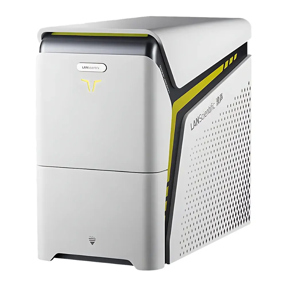
| Brand | LANScientific |
|---|---|
| Origin | Jiangsu, China |
| Manufacturer Type | Direct Manufacturer |
| Origin Category | Domestic (China) |
| Model | SuperSEM N10 |
| Instrument Type | Benchtop SEM |
| Electron Source | Tungsten Filament |
| SEM Class | Entry-Level Tungsten-Filament SEM |
| Max Sample Diameter | 90 mm |
| Max Sample Thickness | 40 mm |
| Stage Travel | X: 25 mm, Y: 25 mm, Z: 30 mm |
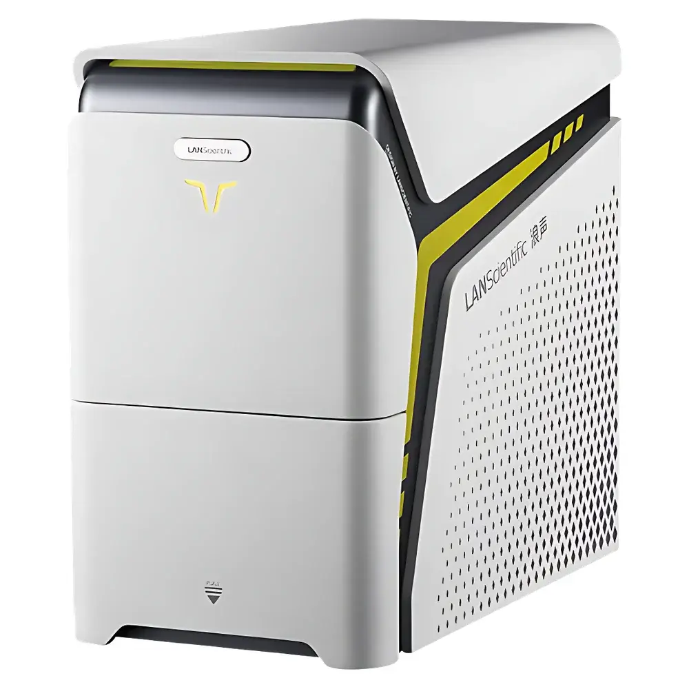
| Brand | LANScientific |
|---|---|
| Origin | Jiangsu, China |
| Manufacturer Type | Direct Manufacturer |
| Country of Origin | Domestic (China) |
| Model | SuperSEM N10eV |
| Instrument Type | Desktop / Benchtop SEM |
| Electron Gun Type | Tungsten Filament |
| Microscope Class | Entry-Level Tungsten-Filament SEM |
| Maximum Sample Dimensions | 90 mm (diameter) × 40 mm (thickness) |
| Stage Travel Range | X: 25 mm, Y: 25 mm, Z: 30 mm |
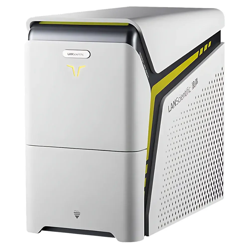
| Brand | LANScientific |
|---|---|
| Origin | Jiangsu, China |
| Manufacturer Type | Direct Manufacturer |
| Region Classification | Domestic (China) |
| Model | SuperSEM N10eX |
| Instrument Type | Desktop SEM |
| Electron Source | Tungsten Filament |
| SEM Class | Entry-Level Tungsten-Filament SEM |
| Maximum Sample Diameter | 90 mm |
| Maximum Sample Thickness | 40 mm |
| Stage Travel | X: 25 mm, Y: 25 mm, Z: 30 mm |
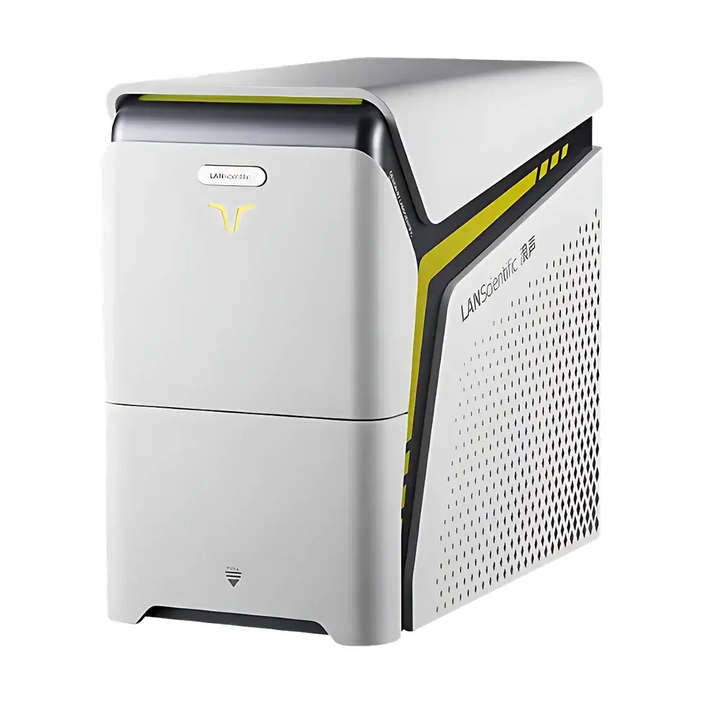
| Brand | LANScientific |
|---|---|
| Origin | Jiangsu, China |
| Manufacturer Type | Direct Manufacturer |
| Regional Category | Domestic (China) |
| Model | SuperSEM N10XL |
| Instrument Type | Desktop SEM |
| Electron Source | Tungsten Filament |
| SEM Class | Entry-Level Tungsten-Filament SEM |
| Sample Chamber Size | Up to 100 × 100 mm |
| Detector Configuration | Secondary Electron Detector (SED), Quadrant Backscattered Electron Detector (BSE), Integrated Silicon Drift Detector (SDD)-based EDS System |
| Real-Time Imaging Mode | Video-rate BSE + EDS spectral acquisition |
| Software Features | Auto-focus, Auto-stigmation, Auto-contrast/brightness, Large-area Stitching, Live EDS Mapping, Real-time Spectral Overlay |
| Power Requirement | Standard AC 220 V, 50 Hz |
| Footprint | < 0.8 m² |
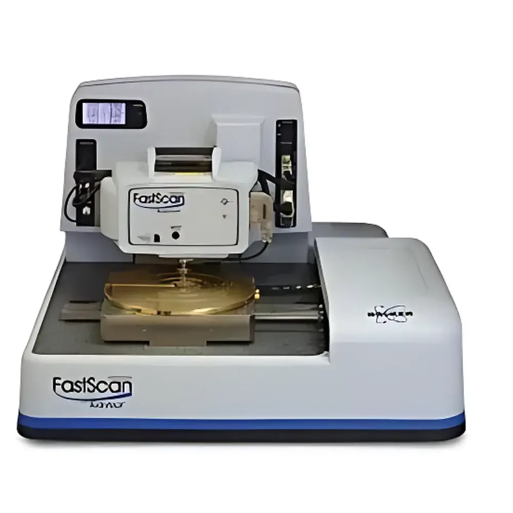
| Brand | Bruker |
|---|---|
| Origin | USA |
| Manufacturer Type | Authorized Distributor |
| Origin Category | Imported |
| Model | Dimension FASTSCAN |
| Pricing | Available Upon Request |
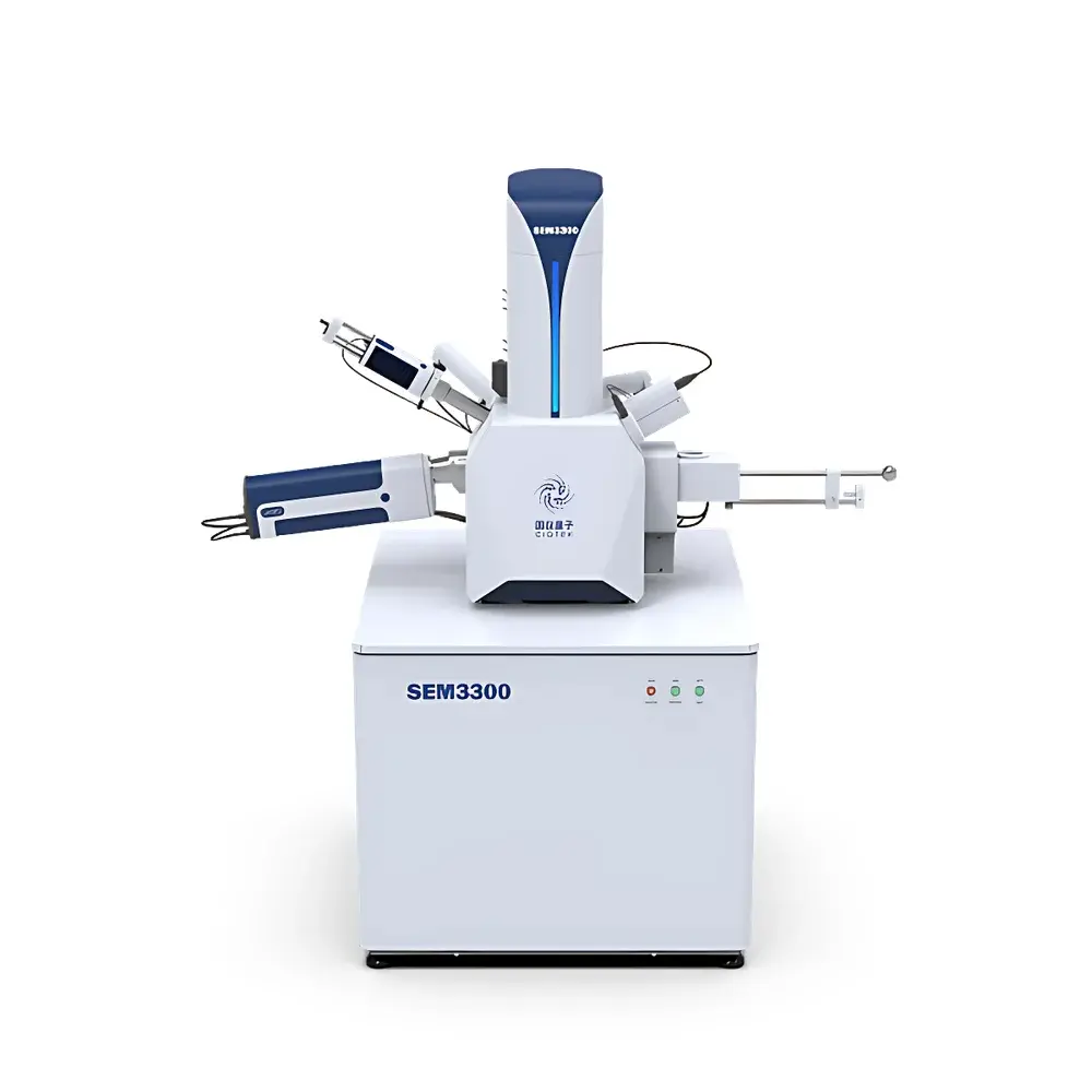
| Brand | CIQTEK |
|---|---|
| Origin | Anhui, China |
| Manufacturer Type | Direct Manufacturer |
| Origin Category | Domestic (China) |
| Model | SEM3300 |
| Instrument Type | Floor-Standing Conventional SEM |
| Electron Source | Tungsten Filament |
| SEM Class | Entry-Level Tungsten-Filament SEM |
| Secondary Electron Resolution | 2.5 nm @ 20 kV |
| Magnification Range | 1× to 300,000× |
| Accelerating Voltage | 0.1 kV to 30 kV |
| Stage Travel | X: 120 mm |
| Y | 115 mm |
| Z | 50 mm |
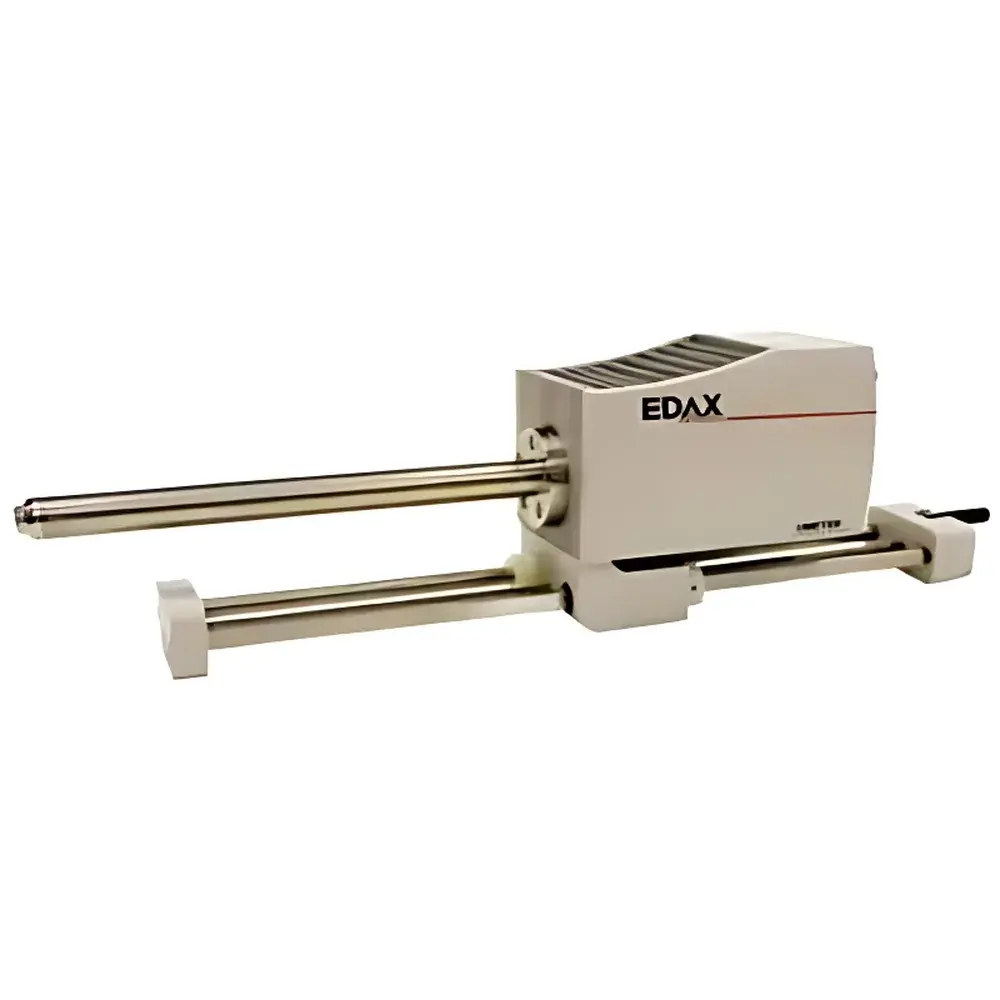
| Origin | USA |
|---|---|
| Manufacturer Type | Authorized Distributor |
| Origin Category | Imported |
| Model | Genesis Apollo X/XL |
| Price Range | USD 68,000 – 136,000 (based on FOB USD conversion) |
| Electron Source Compatibility | Tungsten Filament SEMs |
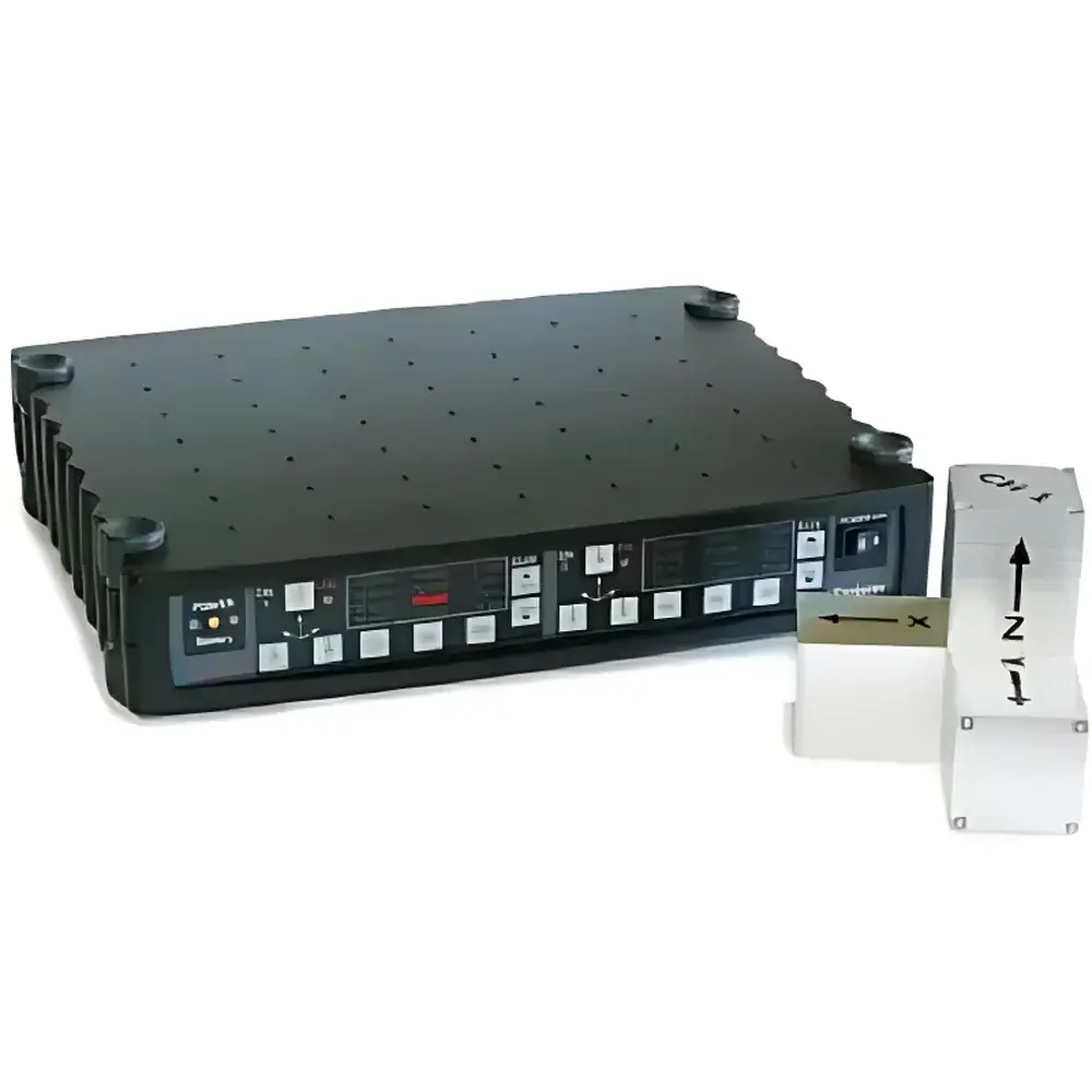
| Brand | Accurion |
|---|---|
| Origin | Germany |
| Model | Halcyonics Explorer |
| Sensor Technology | Piezoelectric Ceramic |
| Axes | X, Y, Z (Triaxial) |
| Detection Principle | Non-contact Capacitive / Laser Doppler (Configurable) |
| Power Supply | Independent AC Input |
| Dual-Sensor Capability | Yes |
| Compliance | CE, RoHS, ISO 10816-1 (Vibration Evaluation of Machines) |
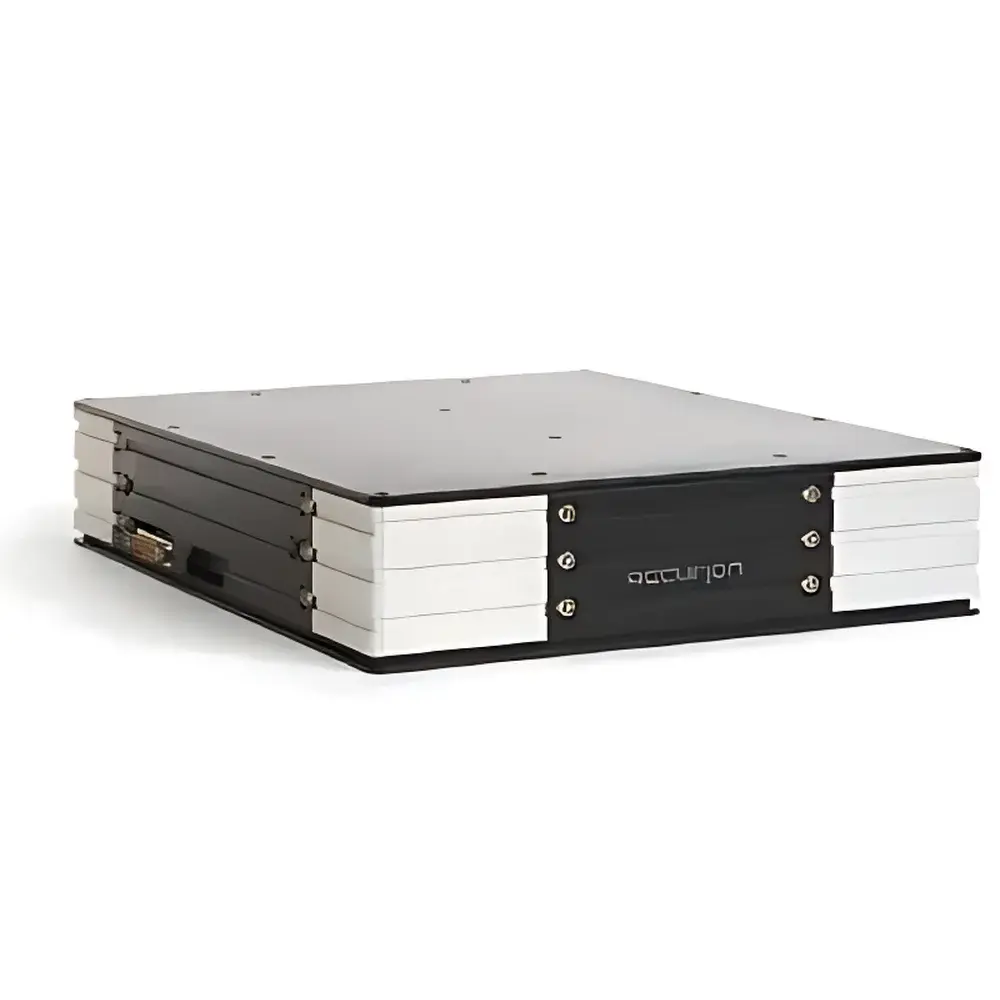
| Brand | Accurion |
|---|---|
| Origin | Germany |
| Manufacturer Type | Authorized Distributor |
| Origin Category | Imported |
| Model | Halcyonics Nano Series Micro Active Vibration Isolation Platform |
| Price | Upon Request |
| Load Capacity | Nano_20: 0–8 kg |
| Nano_30 | 5–25 kg |
| Dimensions | Nano_20: 204 mm × 204 mm × 69 mm |
| Nano_30 | 400 mm × 300 mm × 75 mm |
| Vibration Attenuation Range | 1–200 Hz |
| Resonant Frequency | < 5 Hz |
| Actuation Principle | Piezoelectric Force Feedback |
| Operating Voltage | Low-Voltage DC (Non-Interfering) |
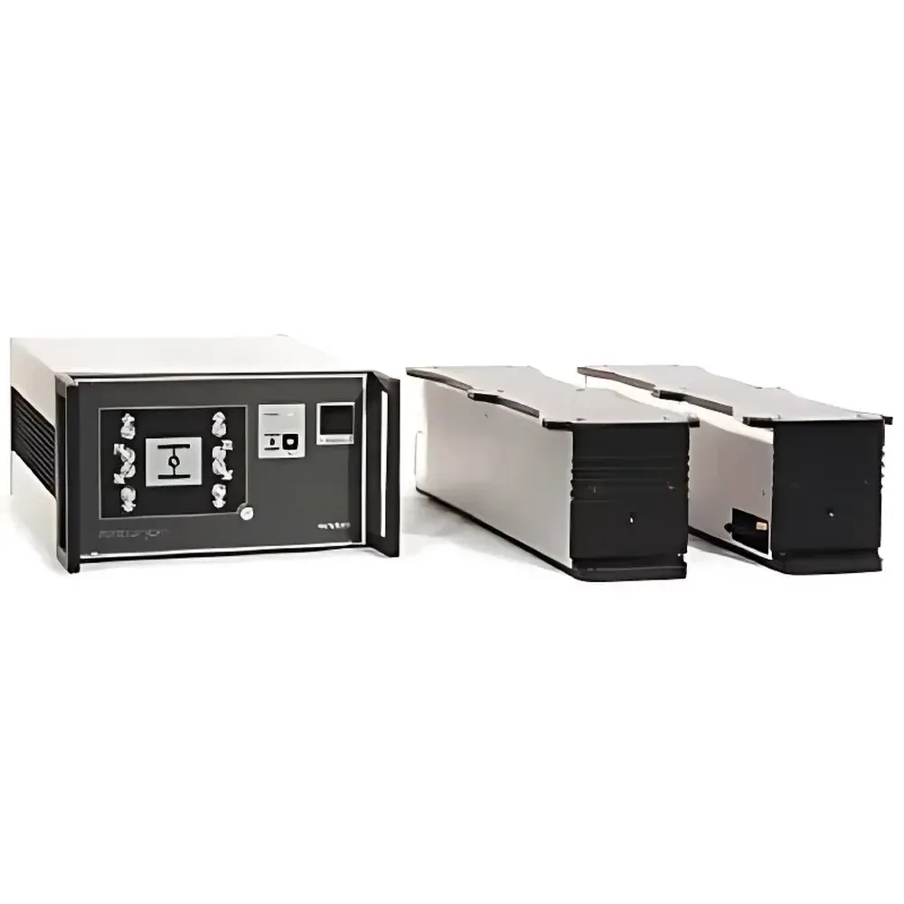
| Brand | Accurion |
|---|---|
| Origin | Germany |
| Manufacturer Type | Authorized Distributor |
| Product Origin | Imported |
| Model | Halcyonics Vario Series |
| Price | Upon Request |
| Load Capacity | 0–600 kg |
| Operating Frequency Range | <5 Hz (effective isolation down to DC) |
| Power Supply | Standard DC Input |
| System Architecture | Separated Actuator Units + Dedicated Controller Unit |
| Key Technology | Piezoelectric Sensor Feedback + Real-Time Active Force Cancellation |
| Compliance | Designed for ISO 20483-compliant lab environments |
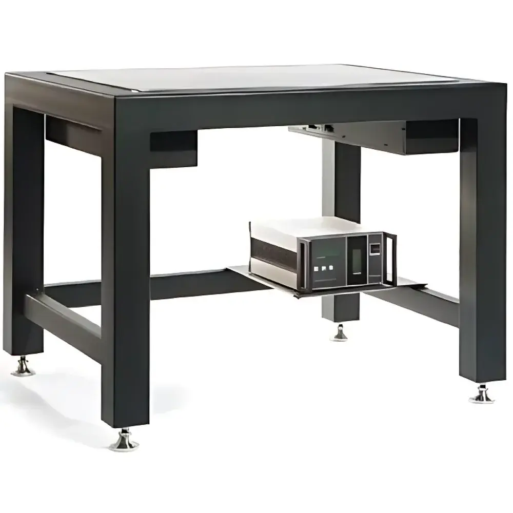
| Brand | Accurion |
|---|---|
| Origin | Germany |
| Model | Halcyonics Workstations Active Vibration Isolation Tables |
| Load Capacity Range | 80–320 kg |
| Isolation Performance | >98.22% at 10 Hz |
| Effective Low-Frequency Cutoff | <5 Hz |
| Interface | USB 1.1 |
| Software | Windows-based Evaluation Suite |
| Dimensions (L×W×H) | 770×770×700 mm to 1070×1170×700 mm |
| Series | Workstation_Vario, Workstation_Micro |
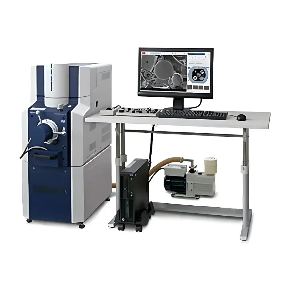
| Brand | Hitachi High-Tech |
|---|---|
| Origin | Japan |
| Manufacturer | Hitachi High-Technologies Corporation |
| Product Type | Imported Desktop SEM |
| Model | FlexSEM 1000 II |
| Electron Source | Tungsten Filament |
| Secondary Electron Resolution | 4.0 nm @ 20 kV (High Vacuum), 15.0 nm @ 1 kV (High Vacuum) |
| Backscattered Electron Resolution | 5.0 nm @ 20 kV (Low Vacuum) |
| Magnification Range | 6×–300,000× (Film Equivalent), 16×–800,000× (Display) |
| Accelerating Voltage | 0.3–20 kV |
| EDS Detector | 30 mm² Silicon Drift Detector (SDD), Nitrogen-free |
| Dimensions (Main Unit) | 450 mm (W) × 640 mm (D) |
| Power Interface | Standard IEC C13 Socket |
| System Architecture | Modular Main Unit + Detachable Power Supply Unit |
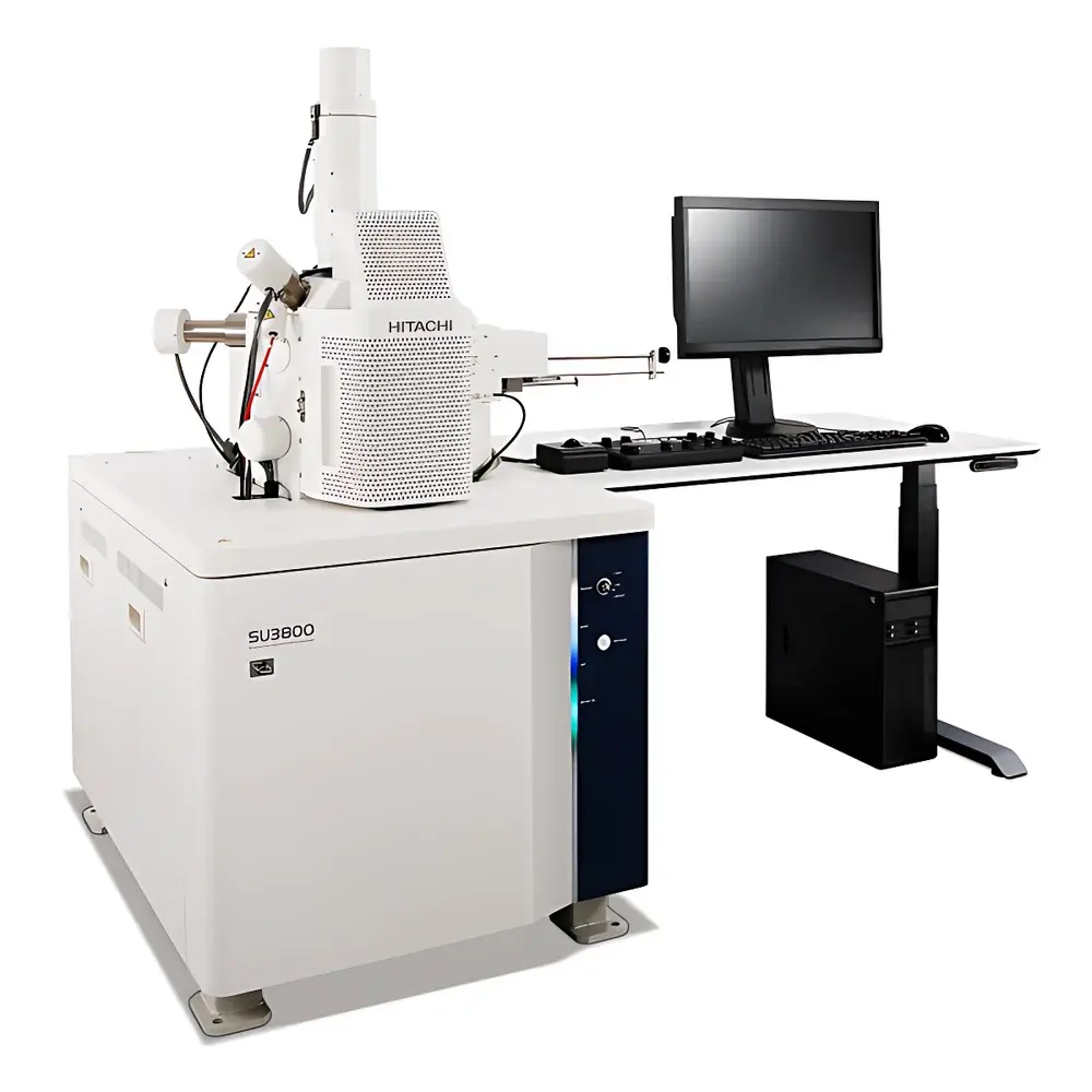
| Brand | Hitachi |
|---|---|
| Origin | Japan |
| Manufacturer Type | Original Equipment Manufacturer (OEM) |
| Import Status | Imported |
| Model | SU3800 |
| Electron Source | Tungsten Filament |
| Secondary Electron Resolution | 3.0 nm at 30 kV |
| Magnification Range | 5–300,000× (low mode), 7–800,000× (high mode) |
| Accelerating Voltage | 0.3–30 kV (standard mode) |
| Backscattered Electron Resolution | 4.0 nm at 30 kV (low-vacuum mode) |
| Maximum Sample Diameter | 200 mm |
| Maximum Sample Height | 80 mm |
| Maximum Sample Weight | 2 kg |
| Navigation System | SEM MAP |
| Automated Imaging | Multi Zigzag Stitching |
| Filament Monitoring | Intelligent Filament Technology (IFT) |
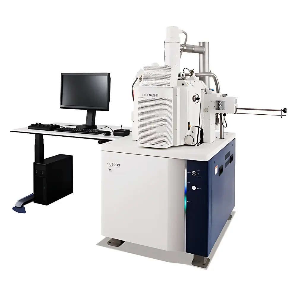
| Brand | Hitachi |
|---|---|
| Origin | Japan |
| Manufacturer | Hitachi High-Tech Corporation |
| Product Type | Imported |
| Model | SU3900 |
| Electron Source | Tungsten Filament |
| Secondary Electron Resolution | 3.0 nm |
| Magnification Range | ×5–300,000 (standard mode), ×7–800,000 (high-magnification mode) |
| Accelerating Voltage | 0.3–30 kV |
| Backscattered Electron Resolution | 4.0 nm @ 30 kV (low-vacuum mode) |
| Maximum Sample Diameter | 300 mm |
| Maximum Sample Height | 130 mm |
| Maximum Sample Weight | 5 kg |
| Navigation Field of View | up to Ø200 mm |
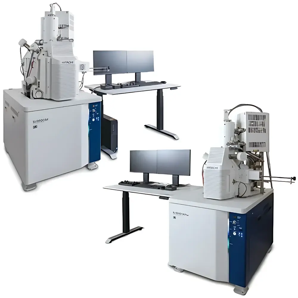
| Brand | Hitachi |
|---|---|
| Origin | Japan |
| Manufacturer Type | Original Equipment Manufacturer (OEM) |
| Product Origin | Imported |
| Model | SU3900/SU3800 SE Series |
| Instrument Type | Floor-Standing Conventional SEM |
| Electron Source | Thermal Field-Emission Gun |
| Secondary Electron Resolution | 0.9 nm @ 30 kV, 2.5 nm @ 1 kV, 1.6 nm @ 1 kV (Deceleration Mode) |
| Magnification Range | ×5 to ×600,000 (Film Equivalent) |
| Accelerating Voltage | 0.5 kV to 30 kV |
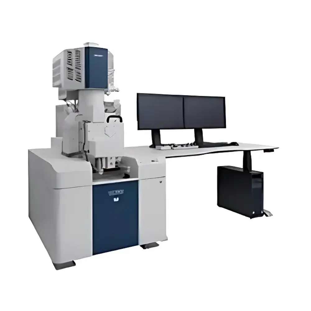
| Brand | Hitachi |
|---|---|
| Origin | Japan |
| Manufacturer | Hitachi High-Tech Corporation |
| Product Type | Imported Instrument |
| Model | SU7000 |
| Electron Gun | Cold Field-Emission (CFEG) |
| Secondary Electron (SE) Resolution | 0.8 nm @ 15 kV, 0.9 nm @ 1 kV |
| Magnification Range | 20× to 2,000,000× |
| Accelerating Voltage | 0.1–30 kV |
| Backscattered Electron (BSE) Resolution | Not Specified |
| Detector Channels | Simultaneous 6-channel signal acquisition and display |
| Maximum Image Resolution | 10240 × 7680 pixels |
| Sample Chamber | Ultra-large chamber with 18 accessory ports |
| Vacuum Mode | High vacuum and low vacuum (down to 300 Pa, optional) |
| Brand | Hitachi |
|---|---|
| Origin | Japan |
| Manufacturer | Hitachi High-Tech Corporation |
| Type | Floor-standing FE-SEM |
| Electron Source | Cold Field-Emission Gun |
| Secondary Electron Resolution | 0.6 nm @ 15 kV |
| Magnification Range | 20× – 2,000,000× |
| Accelerating Voltage | 0.5–30 kV (standard mode) |
| Backscattered Electron Resolution | Not specified |
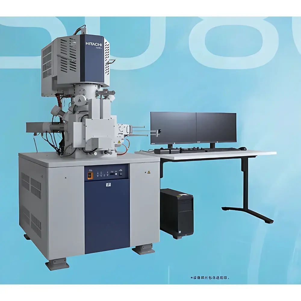
| Brand | Hitachi |
|---|---|
| Origin | Japan |
| Model | SU8600 Series |
| Instrument Type | Floor-Standing SEM |
| Electron Gun | Cold Field Emission |
| Secondary Electron Resolution | 0.6 nm @ 15 kV |
| Magnification Range | 20× to 2,000,000× |
| Accelerating Voltage | 0.5–30 kV |
| Landing Voltage | 0.01–20 kV |
| Maximum Sample Diameter | φ150 mm |
| Detector Options | UD (with ExB energy filter), LD, TD (with energy filter), IMD, PD-BSED, OCD, CLD, STEM Detector |
| Stage | 5-Axis Motorized (X: 0–110 mm, Y: 0–110 mm, Z: 1.5–40 mm, Tilt: −5° to +70°, Rotation: 360°) |
| Software | EM Flow Creator, HD Capture (up to 40,960 × 30,720 px) |
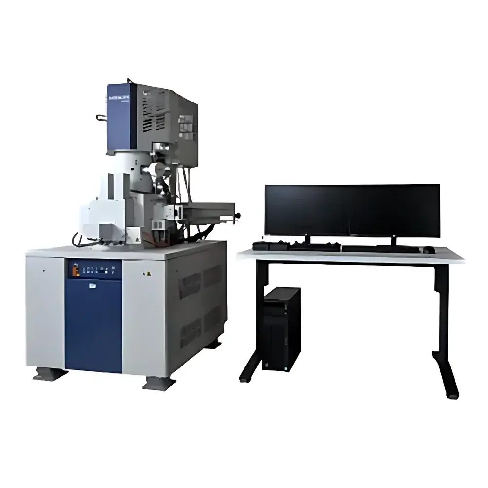
| Brand | Hitachi |
|---|---|
| Origin | Japan |
| Manufacturer | Hitachi High-Tech Corporation |
| Type | Floor-standing SEM |
| Electron Source | Schottky field-emission gun |
| Secondary Electron Resolution | 0.6 nm @ 15 kV, 0.8 nm @ 1 kV, 0.9 nm @ 0.3 kV |
| Magnification Range | 20× – 2,000,000× |
| Accelerating Voltage | 0.1–30 kV (standard mode) |
| Maximum Image Size (optional) | 40,960 × 30,720 pixels |
| Simultaneous Signal Channels | Up to 6 detectors |
| EDS Working Distance Optimization | Short WD configuration enabled via optimized chamber geometry |
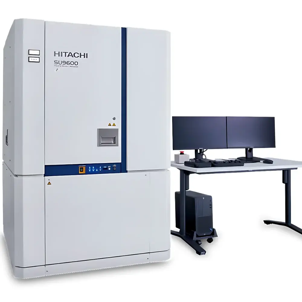
| Brand | Hitachi |
|---|---|
| Origin | Japan |
| Manufacturer | Hitachi High-Tech Corporation |
| Type | Floor-Standing SEM |
| Electron Source | Cold Field-Emission Gun (CFEG) |
| Resolution | 0.6 nm @ 1 kV, 0.4 nm @ 30 kV (Secondary Electron Imaging) |
| Magnification Range | 80× to 3,000,000× |
| Accelerating Voltage | 0.01–30 kV |
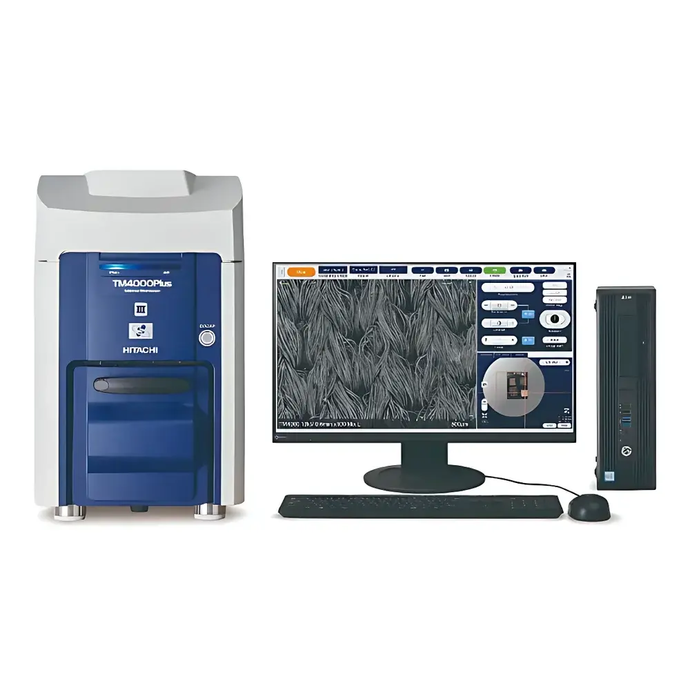
| Brand | Hitachi |
|---|---|
| Origin | Japan |
| Manufacturer Type | Original Equipment Manufacturer (OEM) |
| Product Category | Imported Instrument |
| Model | TM4000PlusIII / TM4000III |
| Instrument Type | Benchtop SEM |
| Electron Source | Tungsten Filament |
| Accelerating Voltage | 5 kV, 10 kV, 15 kV, 20 kV |
| Magnification Range | 10× – 100,000× (photographic magnification) |
| Maximum Sample Diameter | 80 mm |
| Maximum Sample Thickness | 50 mm |
| Stage Travel | X: 40 mm, Y: 35 mm |
| Vacuum Mode | Standard Low-Vacuum Operation |
| Automation Features | Auto-focus, Auto-brightness/contrast, Filament Usage Monitoring, Programmable Workflow Sequencing, Integrated Particle Analysis Support (with Oxford AZtecLiveLite) |
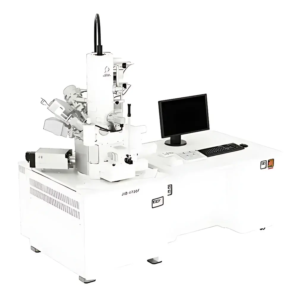
| Brand | JEOL |
|---|---|
| Origin | Japan |
| Model | JIB-4700F |
| Instrument Type | Benchtop Dual-Beam FIB-SEM |
| Electron Source | Cold Field Emission Gun (CFEG) |
| Secondary Electron Resolution | 1.2 nm @ 15 kV, 1.6 nm @ 1 kV |
| Backscattered Electron Resolution | 2.5 nm |
| FIB Resolution | 5 nm @ 30 kV |
| Magnification Range | 25× – 1,000,000× |
| Acceleration Voltage | 0.1–30 kV |
| Maximum FIB Current | 90 nA |
| Maximum SEM Probe Current | 300 nA |
| Gas Injection System | Up to 3 independent channels |
| Sample Stage | 5-axis fully aligned motorized stage |
| Maximum Sample Diameter | 150 mm |
| Sample Loading | Airlock-style exchange |
| Detector Interfaces | EDS, EBSD, STEM, SE/BSE |
| Brand | JEOL |
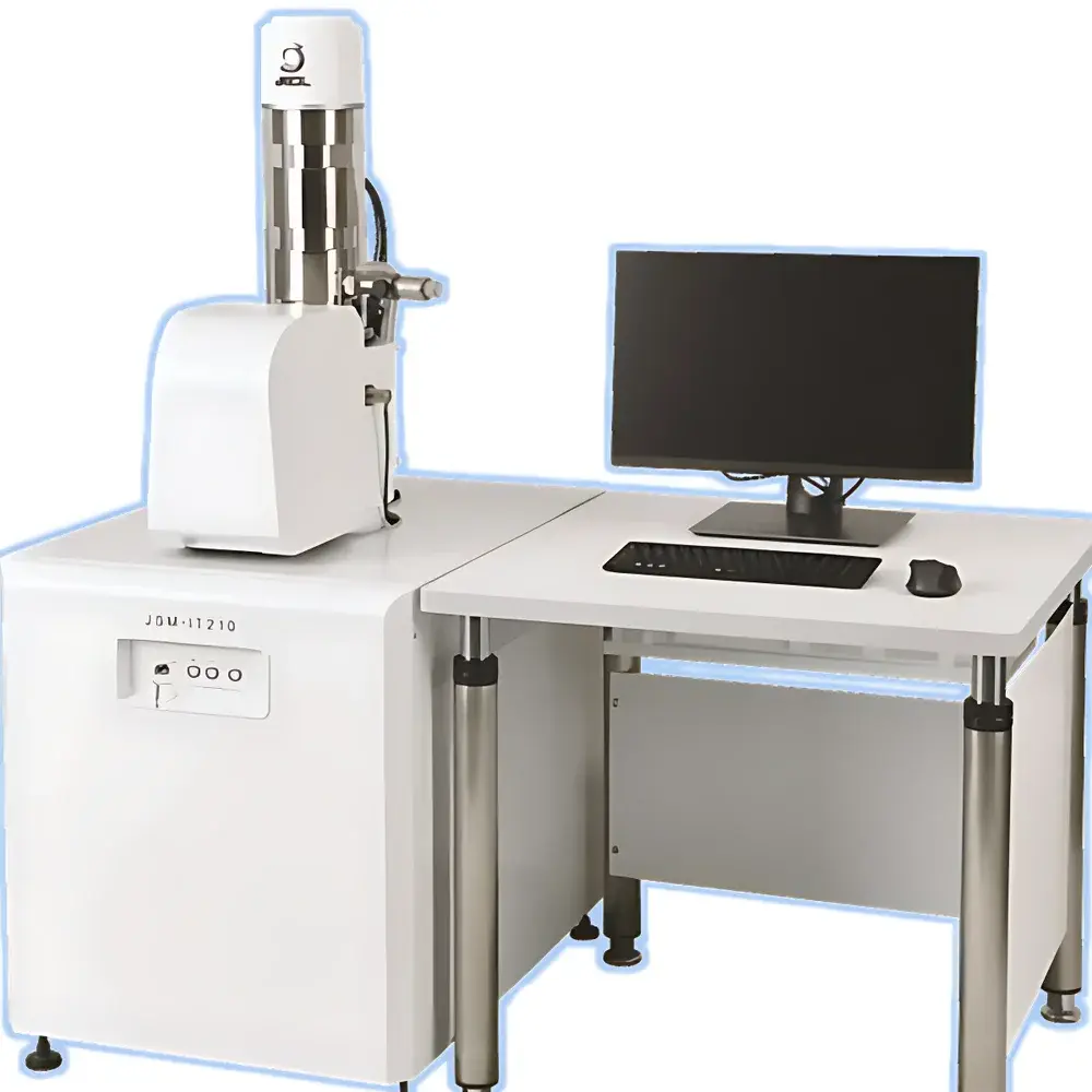
|---|---|
| Origin | Japan |
| Model | JSM-IT210 |
| Instrument Type | Floor-standing |
| Electron Source | Tungsten Filament |
| Secondary Electron Resolution | 3 nm @ 30 kV |
| Magnification Range | 5× – 300,000× |
| Accelerating Voltage | 0.5–30 kV |
| Backscattered Electron Resolution | 4 nm (Low Vacuum Mode) |
| Maximum Sample Dimensions | Ø150 mm × 53 mm height |
| Specimen Chamber Expansion Ports | Multiple |
| Stage Type | Motorized 5-Axis Stage |
| Standard Detectors | Everhart-Thornley SE Detector, Solid-State BSE Detector |
| Brand | JEOL |
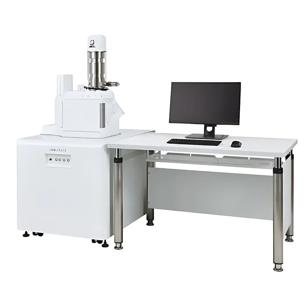
|---|---|
| Origin | Japan |
| Model | JSM-IT510 |
| Instrument Type | Floor-standing SEM |
| Electron Source | Tungsten Filament |
| Secondary Electron Resolution | 3 nm @ 30 kV, 15 nm @ 1 kV |
| Backscattered Electron Resolution | 4 nm @ 30 kV |
| Accelerating Voltage Range | 0.3–30 kV |
| Magnification Range | 14×–800,000× (on display) |
| Vacuum Mode | Low-vacuum compatible with LHSED detector |