
Process Measurement & Detection Equipment
Filter
Showing 1–30 of 83 results
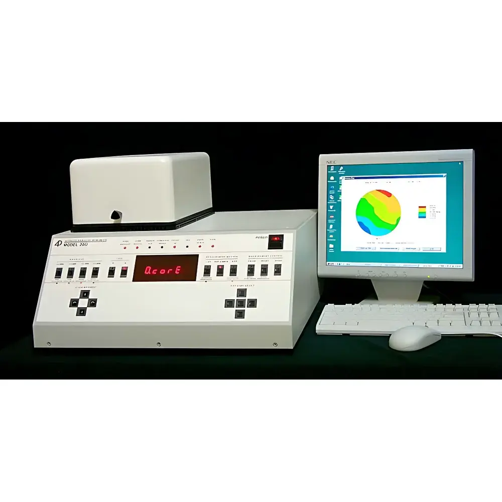
| Brand | 4D TECHNOLOGY |
|---|---|
| Origin | USA |
| Model | 280SI |
| Automation Level | Fully Automatic |
| Sheet Resistance Range | 0.001 Ω/□ to 8×10⁵ Ω/□ (Standard) |
| Sheet Resistance Accuracy | <0.1% |
| Resistivity Range | 0.001 Ω·cm to 8×10⁵ Ω·cm (derived from sheet resistance and user-input film thickness) |
| Resistivity Accuracy | <0.1% |
| Substrate Size Support | 2–8 inch wafers (333-series supports up to 12 inch |
| Test Current Accuracy | <0.1% |
| Probe Force Adjustment Range | 90–200 g |
| Probe Tip Material | Tungsten carbide with sapphire bushings |
| Edge Correction Capability | Yes, within 3 mm from wafer edge |
| Measurement Speed | >45 points/min |
| Repeatability | <0.2% (per substrate) |
| Data Output | 2D/3D contour maps, statistical summaries, Excel-compatible reports |
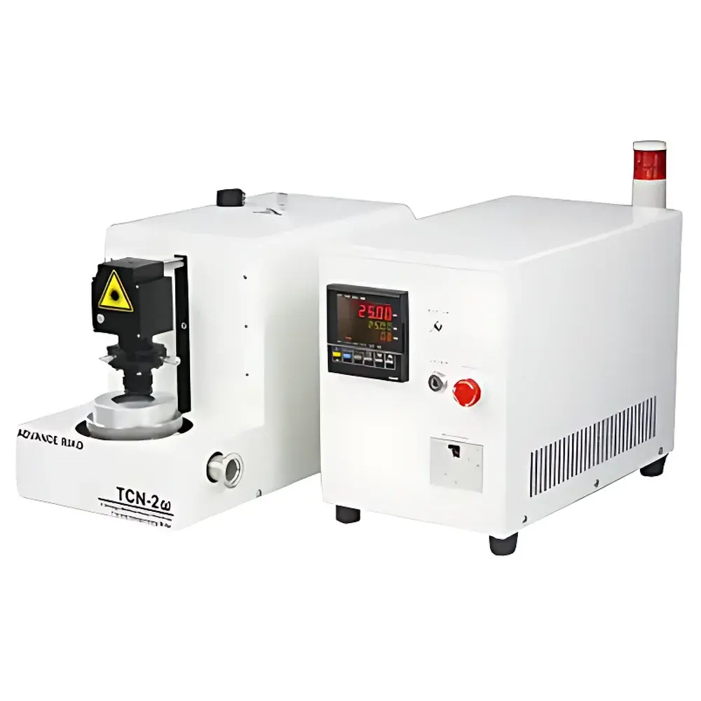
| Brand | ADVANCE RIKO |
|---|---|
| Origin | Japan |
| Model | TCN-2ω |
| Measurement Principle | 2ω Lock-in Thermography (Cross-Plane Thermal Conductivity) |
| Temperature Range | Ambient (23 ± 2 °C) |
| Sample Dimensions | 10–20 mm (L) × 10 mm (W) × 0.3–1 mm (total thickness, including substrate) |
| Substrate Options | Si (recommended), Ge, Al₂O₃ |
| Metal Transducer Film | Au, 100 nm thick, 1.7 mm × 15 mm |
| Thermal Conductivity Range | 0.1–10 W·m⁻¹·K⁻¹ |
| Atmosphere | Ambient air |
| Compliance | ISO/IEC 17025-aligned methodology, compatible with GLP documentation workflows |
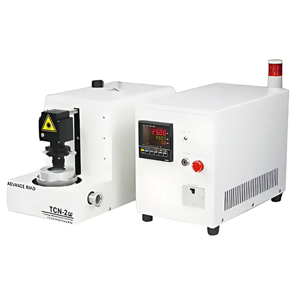
| Brand | ADVANCE RIKO |
|---|---|
| Origin | Japan |
| Model | TCN-2ω |
| Measurement Principle | 2ω Lock-in Thermography (Frequency-Doubled Resistive Heating + Surface Thermal Reflectance Detection) |
| Temperature Range | Ambient (23 ± 2 °C) |
| Sample Dimensions | 10–20 mm (L) × 10 mm (W) × 0.3–1 mm (T, including substrate) |
| Substrate Materials | Si (recommended), Ge, Al₂O₃ |
| Metal Transducer Film | Au, 100 nm thick, 1.7 mm × 15 mm |
| Thermal Conductivity Range | 0.1–10 W·m⁻¹·K⁻¹ |
| Atmosphere | Ambient air |
| Compliance | ASTM E1461 (modified), ISO 22007-2 (principle-aligned), GLP-ready data traceability |
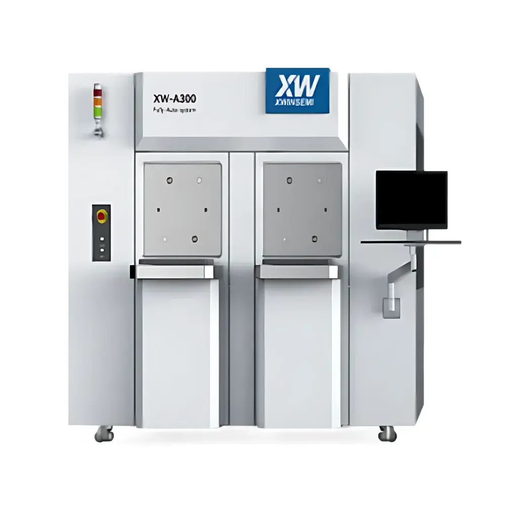
| Brand | Aiyao Instruments |
|---|---|
| Origin | Taiwan |
| Model | XW-A300 |
| Measurement Principles | Spectral Interferometry (IR), White-Light Interferometry (WLI), Optical Reflectometry |
| Sample Compatibility | 4″–12″ wafers |
| Probe Configuration | Single or Dual (top/bottom) |
| Compliance | SEMI S2/S8 |
| Motion Platform | Air-bearing vibration-isolated stage |
| Software | WaferSpect™ with full mapping, statistical analysis, and GLP-compliant audit trail |
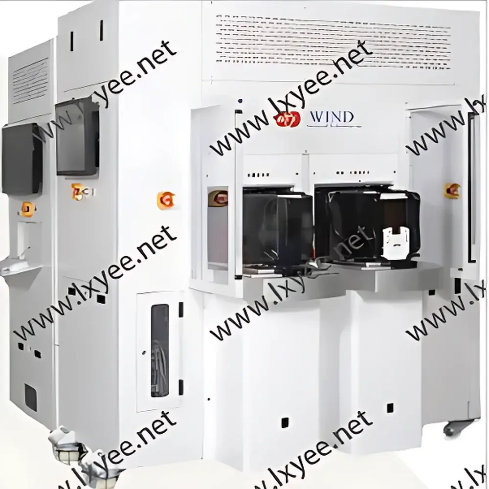
| Brand | ATI |
|---|---|
| Model | WIND |
| Category | Wafer Defect Electron Beam Inspection Equipment |
| Origin | South Korea |
| Frame Material | Hairline Stainless Steel with White Powder Coating |
| Dimensions (W×D×H) | 1900 mm × 1680 mm × 2100 mm |
| Weight | 3.5 tons |
| Wafer Compatibility | 200 mm & 300 mm bare wafers |
| Load Port Support | FOUP, open cassette, ring cassettes (8″, 12″) |
| Alignment | Dual-wafer-size auto-alignment (200/300 mm bare |
| Automation Interface | SECS/GEM compliant, SEMI E84 standard |
| Vision System | Dual-optic 2D/3D module with real-time auto-focus |
| Inspection Modes | Normal/sawing inspection, bump inspection, edge/kerf measurement, 3D bump height/warpage/coplanarity/thickness/BLT metrology |
| Algorithm | Die-to-Die (D2D) registration using optimal die selection from adjacent four dies |
| Optional Module | IR imaging for subsurface crack and silicon bulk defect detection |
| Compliance | Fully aligned with SEMI standards |
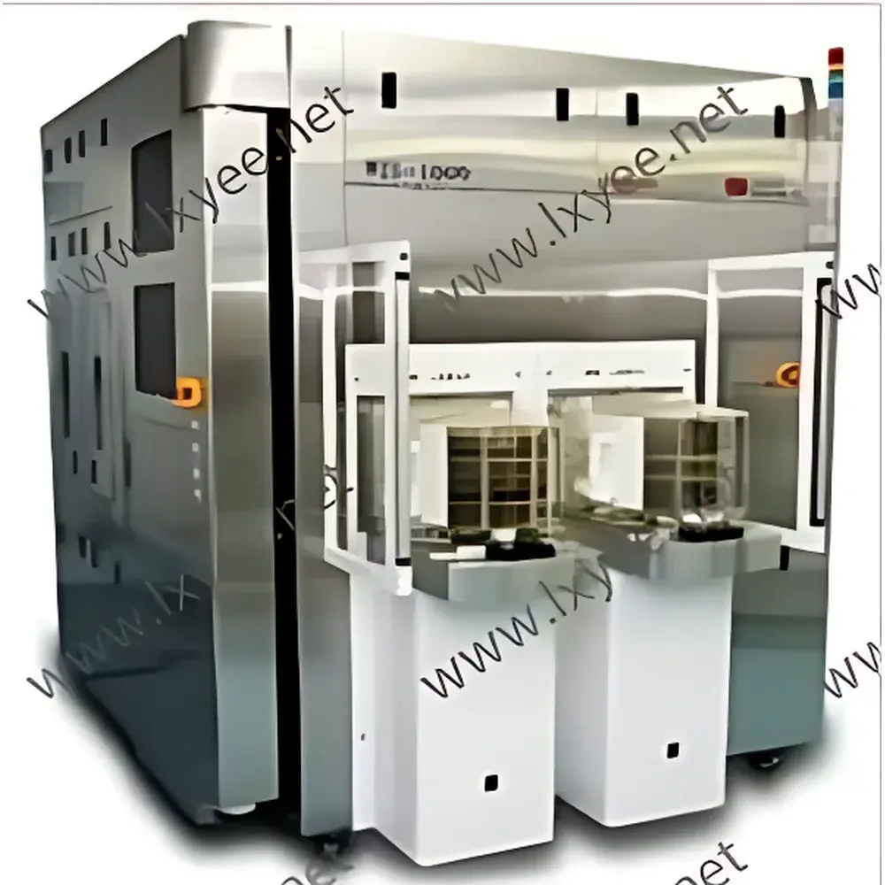
| Brand | ATI |
|---|---|
| Origin | Germany |
| Manufacturer Type | Authorized Distributor |
| Product Category | Imported Instrument |
| Model | WIS-1000 |
| Instrument Type | Optical Patterned Wafer Defect Inspection System |
| Target Applications | Semiconductor Front-End Process Monitoring |
| Process Node Support | Sub-28 nm FinFET and FD-SOI Technologies |
| Compatible Wafer Sizes | 200 mm and 300 mm |
| Throughput | Up to 120 wafers per hour (depending on inspection recipe and defect density) |
| Optical Resolution | ≤ 150 nm (at λ = 405 nm, high-NA dark-field imaging) |
| Defect Detection Sensitivity | ≥ 95% for ≥ 80 nm particles and ≥ 120 nm pattern bridging/bridging defects on metal and dielectric layers |
| Compliance | ISO 9001-certified manufacturing |
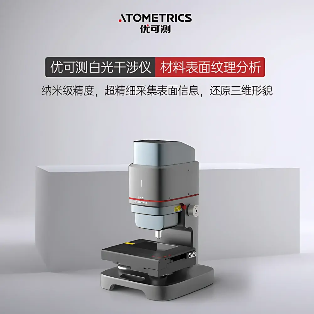
| Brand | Atometrics |
|---|---|
| Origin | Guangdong, China |
| Manufacturer Type | OEM Manufacturer |
| Regional Classification | Domestic (China) |
| Model | AM-7000 Series ER-230 |
| Pricing | Upon Request |
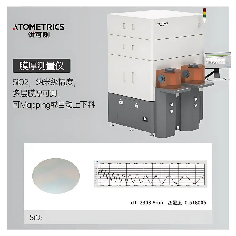
| Brand | Atometrics |
|---|---|
| Origin | Guangdong, China |
| Manufacturer Type | OEM Manufacturer |
| Regional Classification | Domestic (China) |
| Model | T100 |
| Pricing | Upon Request |
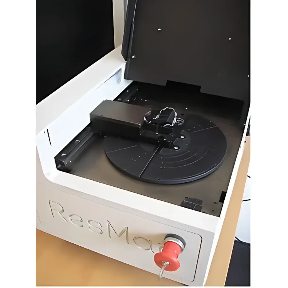
| Brand | CDE ResMap |
|---|---|
| Origin | USA |
| Model | ResMap 168 |
| Automation Level | Fully Automated |
| Probe Material | Tungsten Carbide (WC) |
| Probe Lifetime | >500,000 measurements |
| Vertical Resolution for Probe Contact Optimization | 0.01 mm |
| Measurement Range | 1 mΩ/□ to 5 MΩ/□ |
| Standard Reference Wafers Included | NIST-traceable calibration set (6 pieces) |
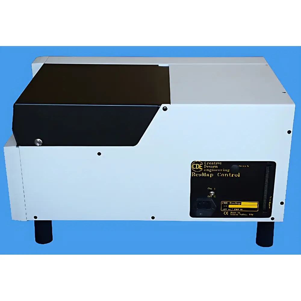
| Brand | CDE (Creative Design Engineering) |
|---|---|
| Model | ResMap 178 |
| Origin | USA |
| Automation Level | Semi-Automatic |
| Measurement Range | 1 mΩ/□ to 5 MΩ/□ |
| Repeatability | ≤ ±0.02% (on static standard resistor) |
| Scan Speed | ≥49 points/min |
| Edge Correction Capability | Effective within 1.5 mm from wafer edge |
| Probe Force Control | Software-adjustable, 90–200 g |
| Probe Types Available | A, B, K, M, N series and custom configurations |
| Supported Substrates | Circular wafers up to 200 mm (8″), square substrates up to 156 mm × 156 mm |
| Data Output | 2D/3D resistivity maps, statistical summaries, Excel-compatible reports |
| Compliance | NIST-traceable calibration standards included (6 certified reference wafers) |
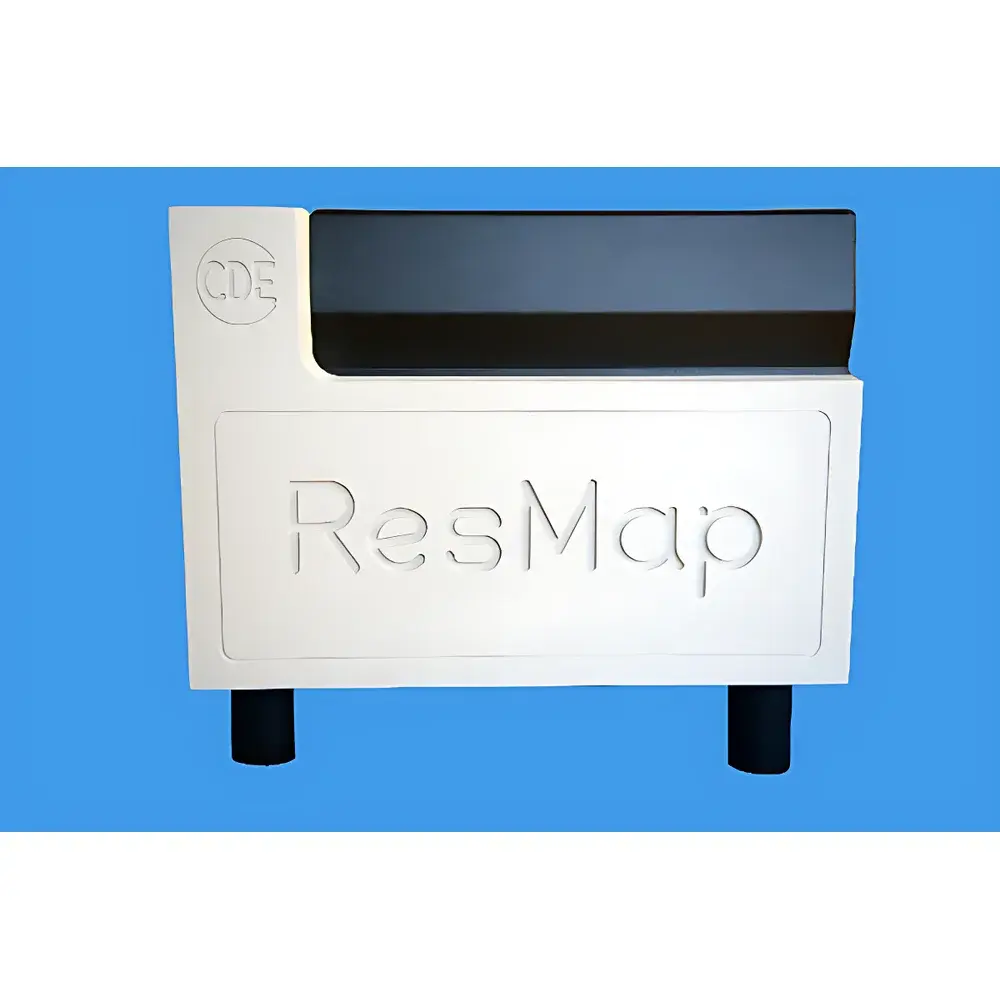
| Brand | CDE ResMap |
|---|---|
| Origin | USA |
| Model | ResMap 273 |
| Automation Level | Fully Automatic |
| Price | USD $68,000 |
| Probe Material | Tungsten Carbide (WC) |
| Probe Lifetime | >500,000 touchdowns |
| Standard Calibration Wafers Included | NIST-traceable set of 6 wafers |
| Measurement Range | 1 mΩ/□ to 5 MΩ/□ |
| Vertical Resolution for Probe Landing Control | 0.01 mm (software-adjustable) |
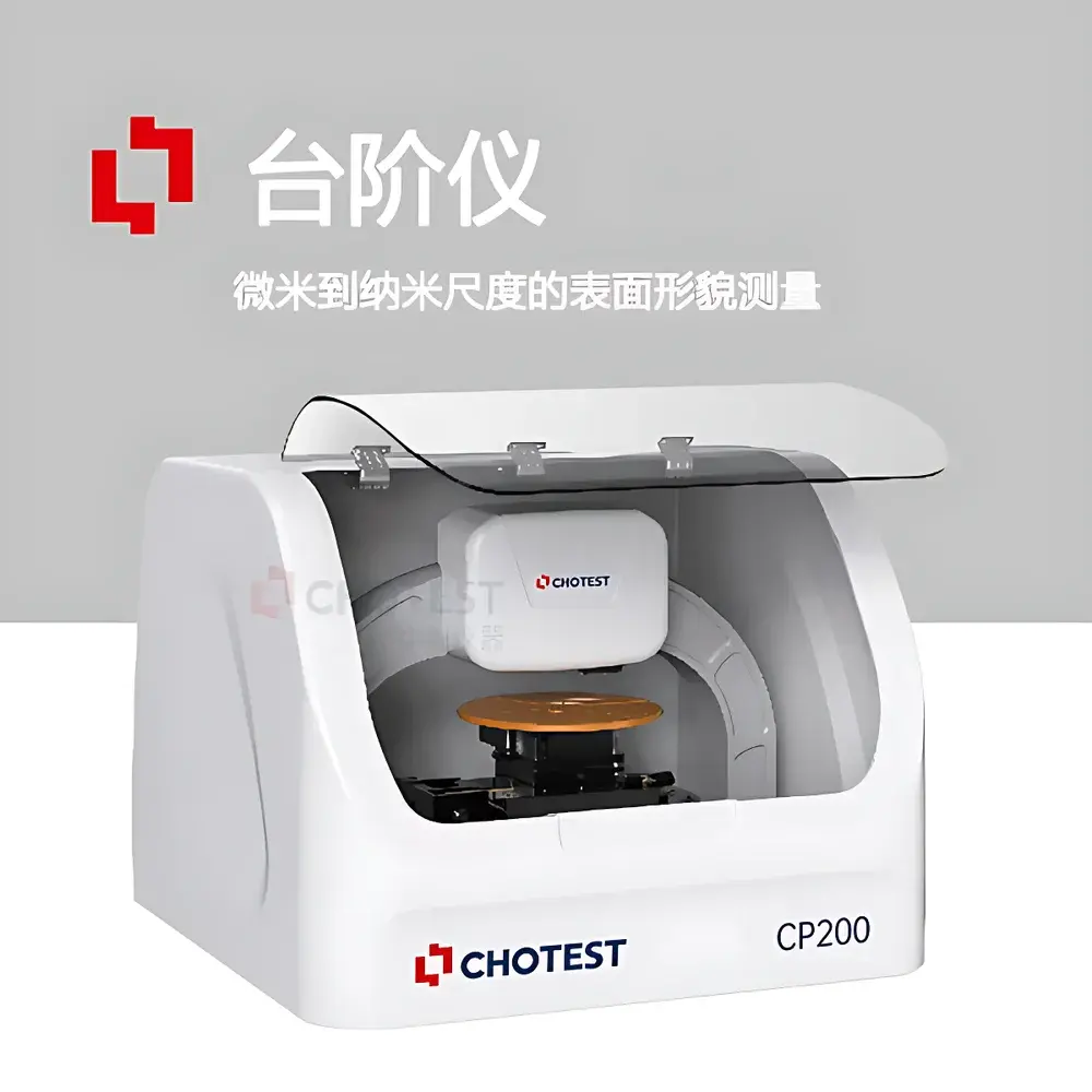
| Brand | Chotest |
|---|---|
| Origin | Guangdong, China |
| Manufacturer Type | Authorized Distributor |
| Country of Origin | China |
| Model | NS200 |
| Price | USD 84,000 (FOB Shenzhen) |
| Measurement Principle | Contact-mode stylus profilometry with LVDC capacitive transduction |
| Vertical Resolution | Sub-ångström (≤0.1 Å) |
| Lateral Scan Range | 55 mm |
| X/Y Stage Travel | 150 mm × 150 mm (motorized) |
| R-θ Stage | 360° continuous motorized rotation |
| Max Sample Thickness | 50 mm |
| Wafer Compatibility | 150 mm (6″) and 200 mm (8″) |
| Vertical Measurement Range | Up to 1000 µm |
| Force Control | 1–50 mg adjustable, electromagnetic micro-force actuation |
| Probe Tip Radius | 2 µm diamond |
| Optical Navigation | 5 MP color camera with real-time probe trajectory overlay |
| SPC Module | Integrated statistical process control with trend charts, Cp/Cpk, histogram, and outlier detection |
| Environmental Requirements | 16–25 °C (ΔT < 2 °C/h), 30–40% RH (non-condensing), floor vibration ≤ 6.35 µm/s (1–100 Hz), ambient noise ≤ 80 dB, laminar airflow ≤ 0.508 m/s downward |
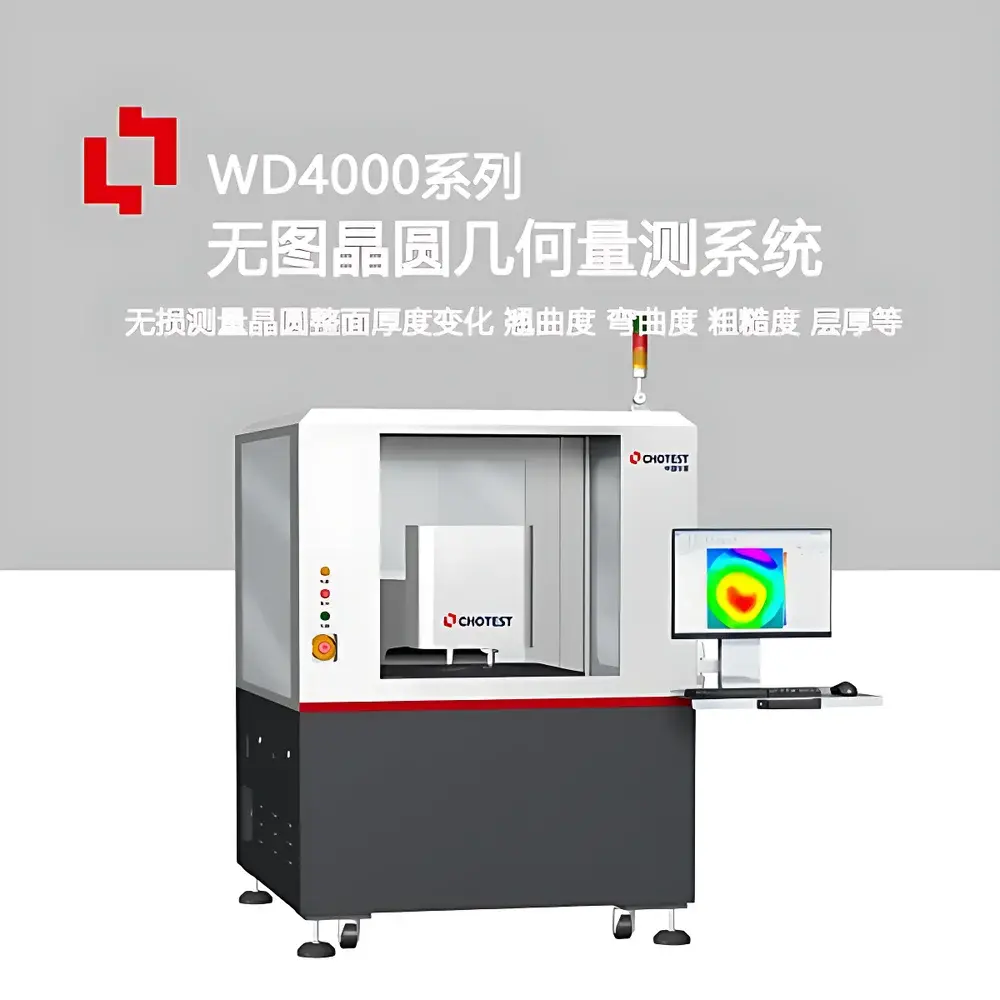
| Brand | Chotest |
|---|---|
| Origin | Guangdong, China |
| Manufacturer Type | Authorized Distributor |
| Country of Origin | China |
| Model | WD4000 |
| Price | USD 420,000 (FOB Shenzhen) |
| Thickness Range | 150 µm – 2000 µm |
| TTV/Bow/Warp Measurement Accuracy | ±0.1 µm (typical, calibrated per ISO 21287) |
| Z-Axis Resolution (Interferometry) | ≤ 0.1 nm |
| Lateral Scan Area | 400 mm × 400 mm |
| Vertical Travel | 75 mm |
| Maximum Wafer Size | 300 mm (12″) |
| Surface Reflectivity Range | 0.05% – 100% |
| Roughness RMS Repeatability | ≤ 0.005 nm (ISO 25178-6 compliant) |
| Interferometric Objective Options | 2.5×, 5×, 10×, 20×, 50× |
| Spectral Confocal Thickness Sensor | Dual-beam, high-stability SLED source, 90 µm measurement range (n = 1.5), minimum detectable thickness: 0.4 µm |
| Infrared Interferometry Module | SLED source, 37–1850 µm range |
| Scan Modes | Full-map, cross (‘X’), star (‘+’), user-defined multi-point |
| Compliance | ISO 5725 (accuracy & precision), ISO 25178-2 (areal texture), ISO 10110-7 (optical surface form), SEMI D39 (wafer geometry), ASTM F39 (silicon wafer bow/warp) |
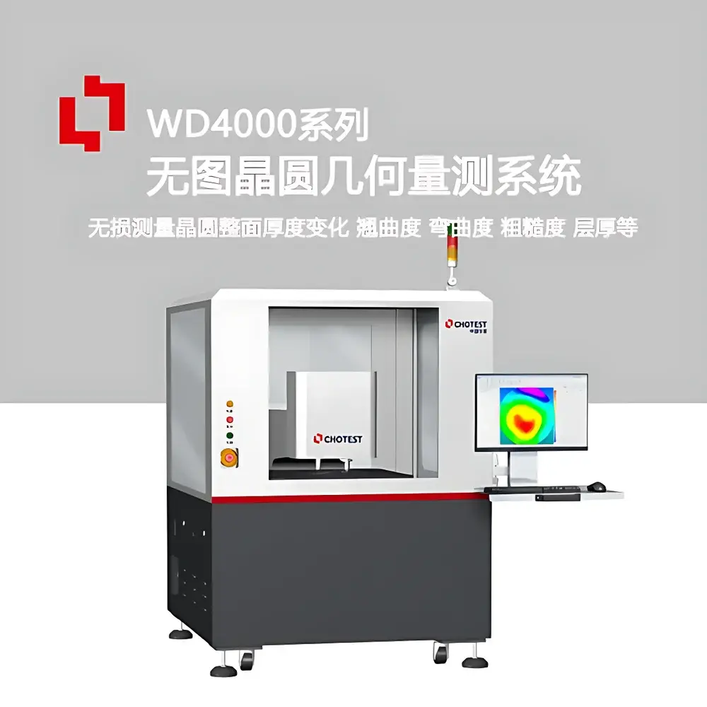
| Brand | Chotest |
|---|---|
| Origin | Guangdong, China |
| Model | WD4000 |
| Thickness Range | 150 µm – 2000 µm |
| 3D Surface Topography Resolution (Z) | ≤ 0.1 nm |
| Roughness RMS Repeatability | ±0.005 nm |
| Supported Wafer Sizes | 4″, 6″, 8″, 12″ |
| Optical Principle | Spectral Confocal Dual-Side Scanning + White-Light Interferometry (WLI) |
| Max XY Travel | 400 mm × 400 mm |
| Z Travel | 75 mm |
| Scan Modes | Full-map, Cross (‘+’), Custom Multi-point |
| Interferometric Objective Options | 2.5×, 5×, 10×, 20×, 50× |
| Reflectivity Range | 0.05% – 100% |
| Film Thickness Range (IR Interferometry) | 37 µm – 1850 µm (n ≈ 1.5) |
| Minimum Detectable Film Thickness | 0.4 µm |
| Vacuum Chuck | ESD-Safe Perforated Ceramic Vacuum Stage |
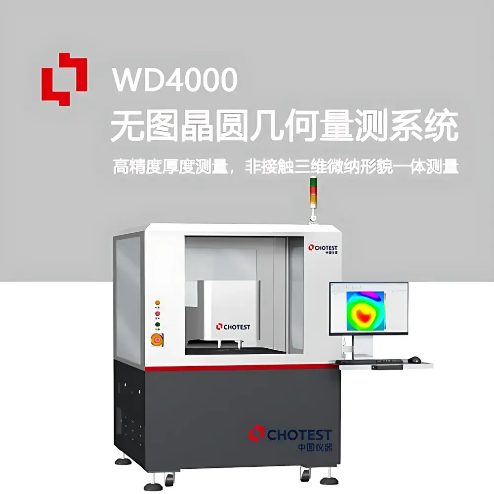
| Brand | Chotest |
|---|---|
| Origin | Guangdong, China |
| Model | WD4000 |
| Measurement Principles | Spectral Confocal Reflectometry (thickness), White-Light Interferometry (3D topography) |
| Wafer Compatibility | 4″–12″ |
| Max. Scan Area | 400 mm × 400 mm |
| Z-Axis Resolution | ≤ 0.1 nm |
| Thickness Range | 150 µm – 2000 µm |
| Surface Reflectivity Range | 0.05% – 100% |
| Roughness RMS Repeatability | ±0.005 nm |
| Motion Stage | Granite-based龙门 with AC servo direct-drive & 0.1 µm encoder resolution |
| Environmental Isolation | Active vibration damping for sub-nm stability |
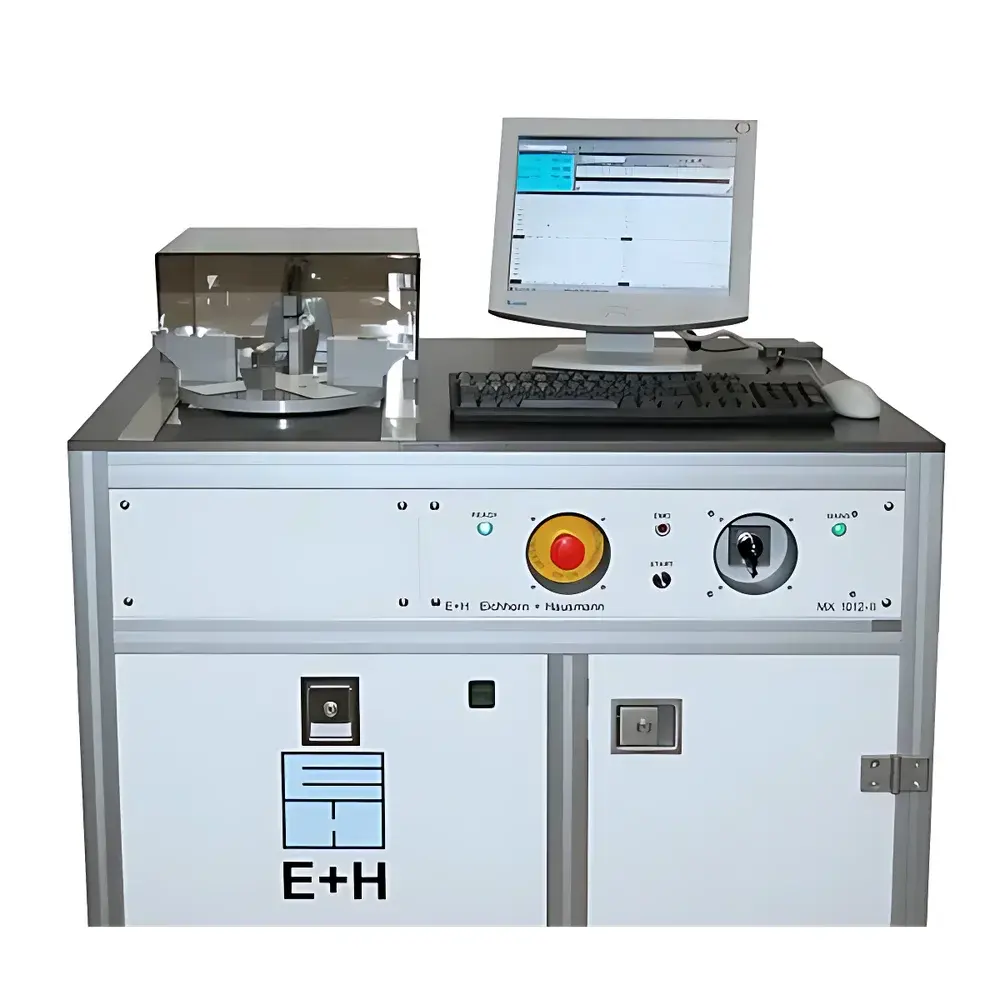
| Brand | E+H Metrology |
|---|---|
| Origin | Germany |
| Manufacturer Type | Authorized Distributor |
| Origin Category | Imported |
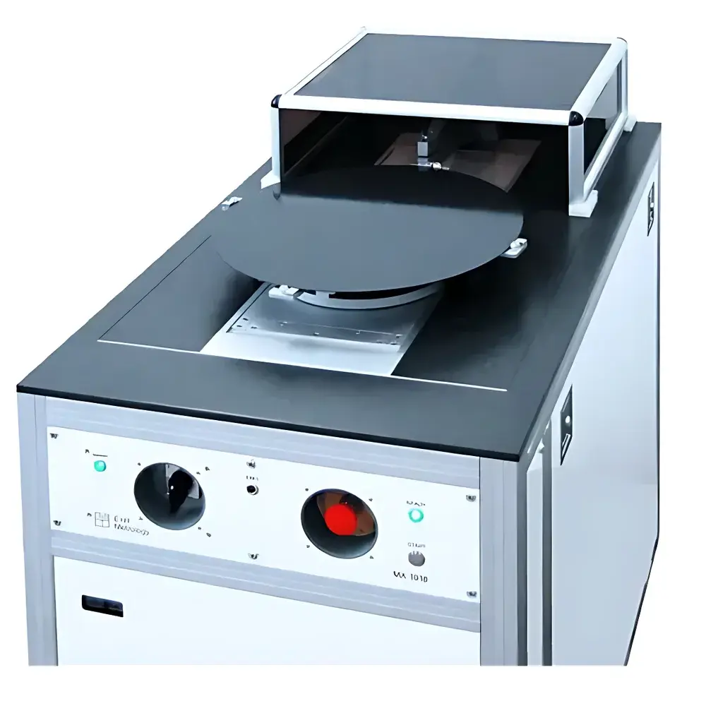
| Model | MX 1012 |
| Pricing | Upon Request |
| Wafer Diameter | 200 mm, 300 mm |
| Accuracy | ±0.1 µm |
| Resolution | 10 nm |
| Spatial Resolution | 1 mm |
| Max Scan Passes | 8 |
| Software | MX-NT |
| Brand | E+H Metrology |
|---|---|
| Origin | Germany |
| Manufacturer Type | Authorized Distributor |
| Origin Category | Imported |
| Model | MX 1018 |
| Pricing | Upon Request |
| Wafer Diameters | 200 mm, 300 mm, 450 mm |
| Measurement Accuracy | ±0.3 µm |
| Vertical Resolution | 10 nm |
| Lateral Spatial Resolution | 1 mm |
| Scan Profiles | Up to 8 radial scans (standard: 4 at 45° intervals) |
| Software Platform | MX-NT |
| Measurement Types | Single-point thickness, full-surface TTV, bow, warp, site flatness |
| Brand | E+H Metrology |
|---|---|
| Origin | Germany |
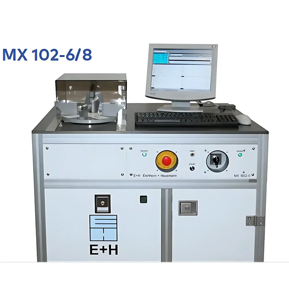
| Model | MX 102-6 / MX 102-8 |
| Wafer Diameter Support | 100 mm, 125 mm, 150 mm, 200 mm |
| Measurement Accuracy | ±0.1 µm |
| Resolution | 10 nm |
| Spatial Resolution | 1 mm |
| Scan Profiles | 4 radial profiles at 45° intervals |
| Software | MX-NT |
| Application | Thickness & TTV metrology post-grinding and post-lapping |
| Brand | E+H Metrology |
|---|---|
| Origin | Germany |
| Manufacturer Type | Authorized Distributor |
| Origin Category | Imported |
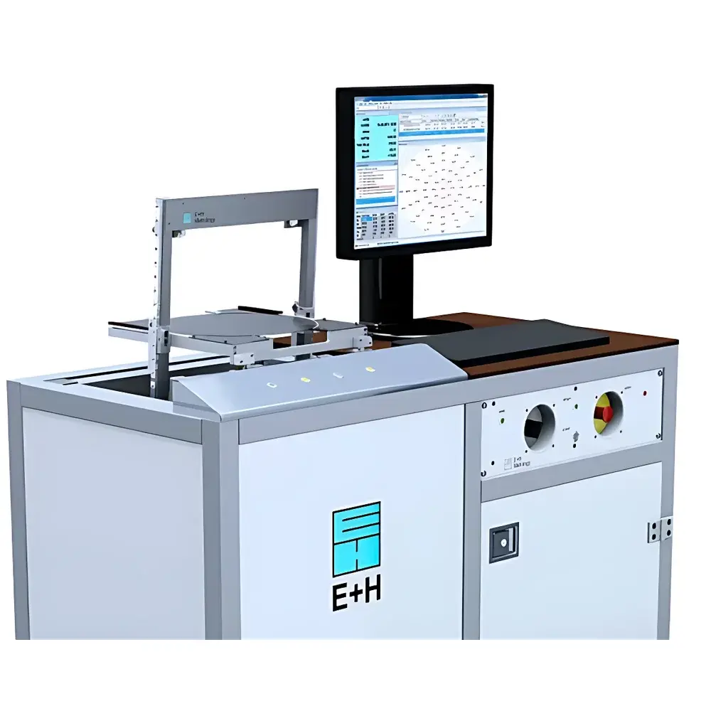
| Model | MX 2012 |
| Pricing | Available Upon Request |
| Wafer Diameter | 300 mm (configurable for 200 mm) |
| Measurement Accuracy | ±0.5 µm |
| Resolution | 50 nm |
| Thickness Range | 500–1000 µm |
| Measurement Points | 69 |
| TTV (Total Thickness Variation) | Supported |
| Bow & Warp | Supported |
| Stress Evaluation | Optional |
| Measurement Orientation | Vertical (gravity-compensated) |
| Automation Level | Semi-automated (manual load/unload, automated measurement cycle) |
| Software | MX-NT |
| Sensor Principle | Capacitive displacement sensing |
| Probe Architecture | Dual orthogonal aluminum plates (1″ thick), each embedded with 69 capacitive sensors |
| Positioning Repeatability | ≤0.1 µm |
| Vacuum Fixture | Triple-circuit independent vacuum suction with dielectric-compensated polymer membrane |
| Brand | E+H Metrology |
|---|---|
| Origin | Germany |
| Manufacturer Type | Authorized Distributor |
| Origin Category | Imported |
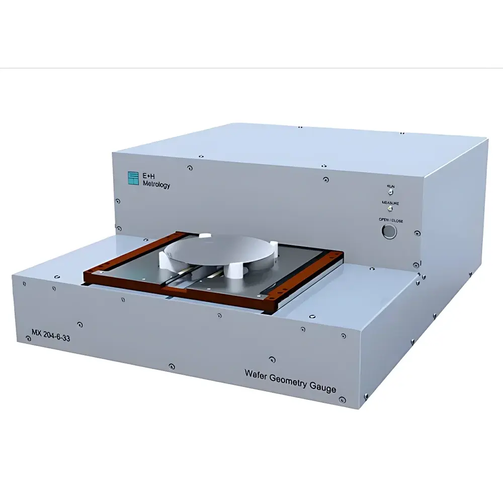
| Model | MX 204 |
| Pricing | Available Upon Request |
| Wafer Diameter | 100 mm, 125 mm, 150 mm, 200 mm, 300 mm |
| Thickness Accuracy | ±0.5 µm to ±1.0 µm |
| Thickness Resolution | 75 nm to 1.0 µm |
| Thickness Range | 100–1000 µm |
| Measurement Principle | Dual-Sided Capacitive Sensing |
| Measured Parameters | Thickness, Total Thickness Variation (TTV), Bow, Warp, Surface Flatness, Stress-Induced Deformation |
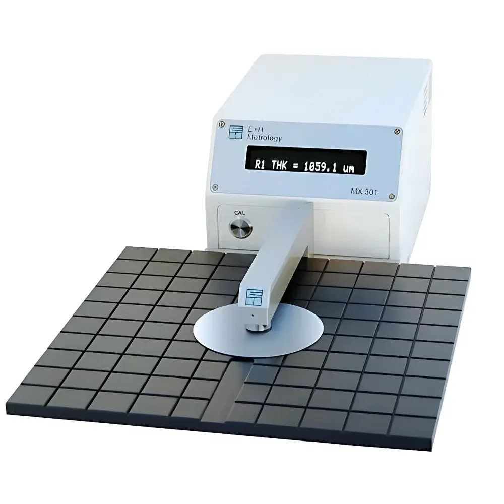
| Brand | E+H Metrology |
|---|---|
| Origin | Germany |
| Model | MX 301 |
| Wafer Diameters Supported | 50 mm, 75 mm, 100 mm, 150 mm, 200 mm, 300 mm |
| Thickness Accuracy | ±0.5 µm |
| Resolution | 10 nm |
| Dynamic Range | 800 µm |
| Standard Thickness Range | 0–1600 µm |
| Measurement Principle | Dual-Sided Capacitive Distance Sensing |
| Calibration Method | Certified Gauge Blocks |
| Output Interface | RS-232 Serial Interface |
| Display | 5-Digit LED |
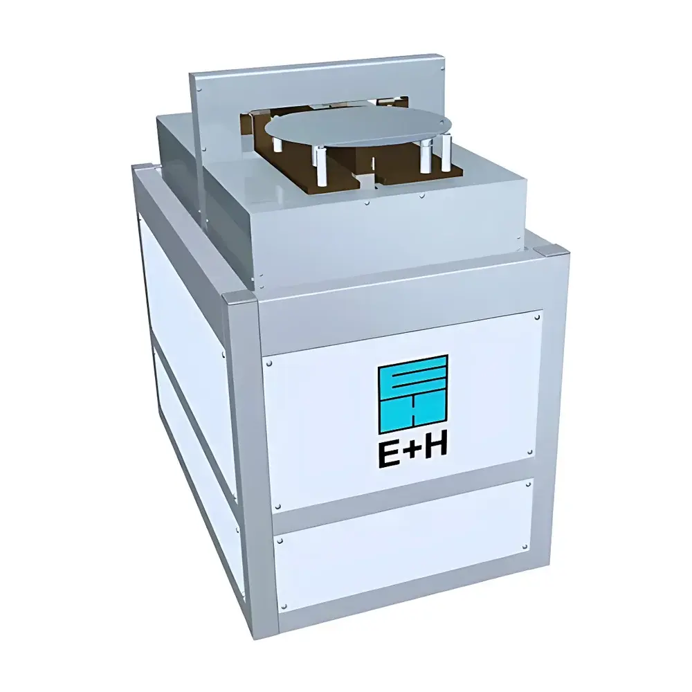
| Brand | E+H Metrology |
|---|---|
| Origin | Germany |
| Manufacturer Type | Authorized Distributor |
| Origin Category | Imported |
| Model | MX 7012 |
| Pricing | Upon Request |
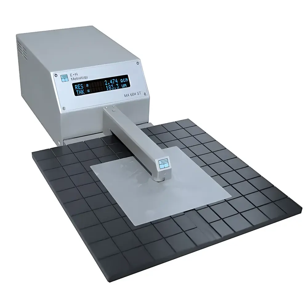
| Brand | E+H Metrology |
|---|---|
| Origin | Germany |
| Model | MX 604-ST |
| Wafer Diameter | 50–200 mm |
| Thickness Range | 60–300 µm or 250–750 µm |
| Thickness Accuracy | ±1 µm |
| Sensor Active Diameter | 8 mm |
| Sensor Housing Diameter | 20 mm |
| Edge Exclusion Distance | 10 mm |
| Measurement Time per Point | 0.3 s |
| Sheet Resistance Range | 10–2000 Ω/sq |
| Resistivity Range | 0.25–50 Ω·cm (at 250 µm) / 0.75–150 Ω·cm (at 750 µm) |
| Software | EHMaster |
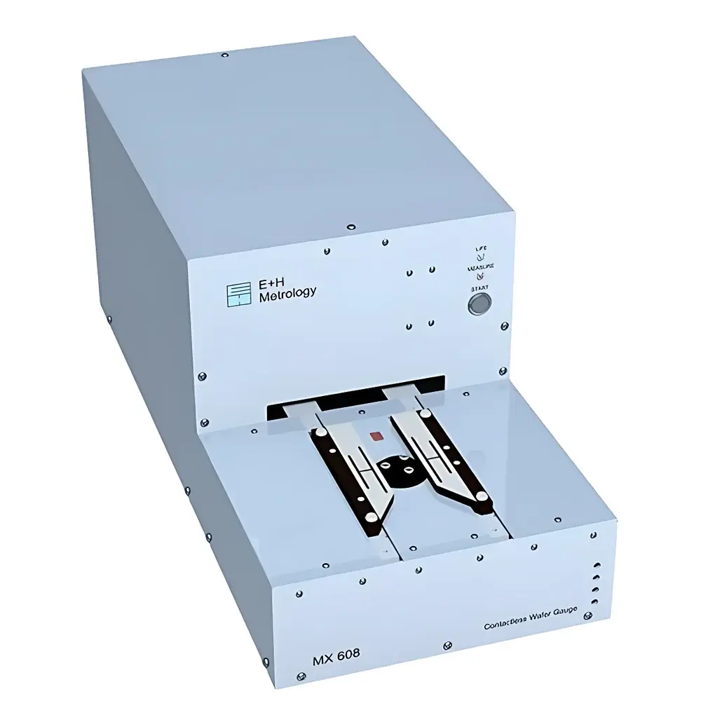
| Brand | E+H Metrology |
|---|---|
| Origin | Germany |
| Model | MX 608 |
| Wafer Sizes Supported | 4", 5", 6", 8" |
| Thickness Range | 300–800 µm (standard 500–800 µm) |
| Max. Warp | 100 µm |
| Resistivity Range | 0.001–200 Ω·cm |
| Thickness Accuracy | ±0.3 µm |
| TTV Accuracy | ±0.1 µm |
| Thickness Resolution | ±0.05 µm |
| Resistivity Accuracy | ±1% (0.001–30 Ω·cm), ±2% (30–100 Ω·cm), ±5% (100–200 Ω·cm) |
| Measurement Time | 7 s (single-point center), 10 s (full radial scan, 180 points on 8″ wafer), ~3 min (18 angular scans × 180 points = 3240-point full mapping) |
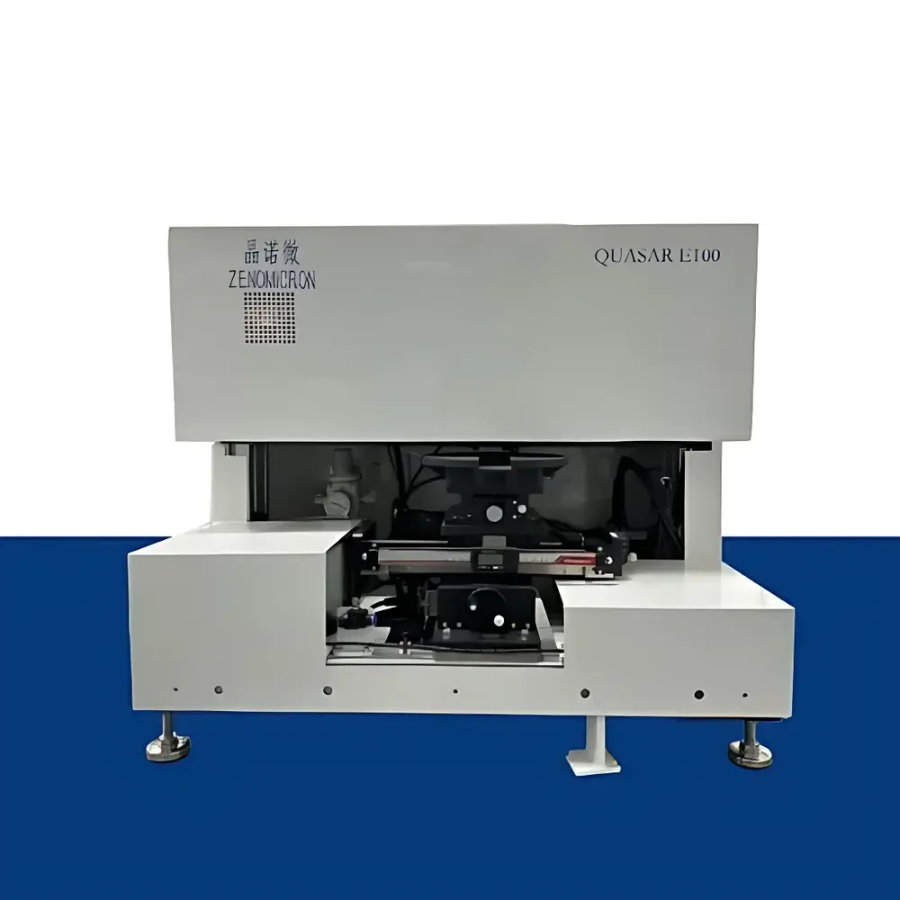
| Brand | ZENO |
|---|---|
| Model | E100 |
| Type | Spectroscopic Ellipsometer |
| Form Factor | Benchtop |
| Measurement Principle | Null- and Rotating-Analyzer-Based Spectroscopic Ellipsometry (SE) |
| Wavelength Range | 240–1700 nm (configurable UV-VIS-NIR) |
| Spot Size | Standard 3 mm Ø |
| Substrate Compatibility | 4″ to 12″ wafers, irregular shapes, rigid/flexible substrates |
| Measured Parameters | Film thickness (sub-nm resolution), complex refractive index (n + ik), extinction coefficient (k), interfacial roughness, optical bandgap |
| Precision | ≤0.01 nm RMS repeatability on SiO₂/Si reference samples (t < 30 nm, n=30 measurements) |
| Compliance | ASTM F1599, ISO 15632, SEMI MF1530 |
| Software | ZENO-EllipSuite v4.x with GLP-compliant audit trail, user role management, and 21 CFR Part 11-ready data export |
| Automation Options | Motorized XYZ stage, auto-alignment module, wafer handler integration |
| Origin | Shanghai, China |
| Distribution | Authorized Global Distributor Network |
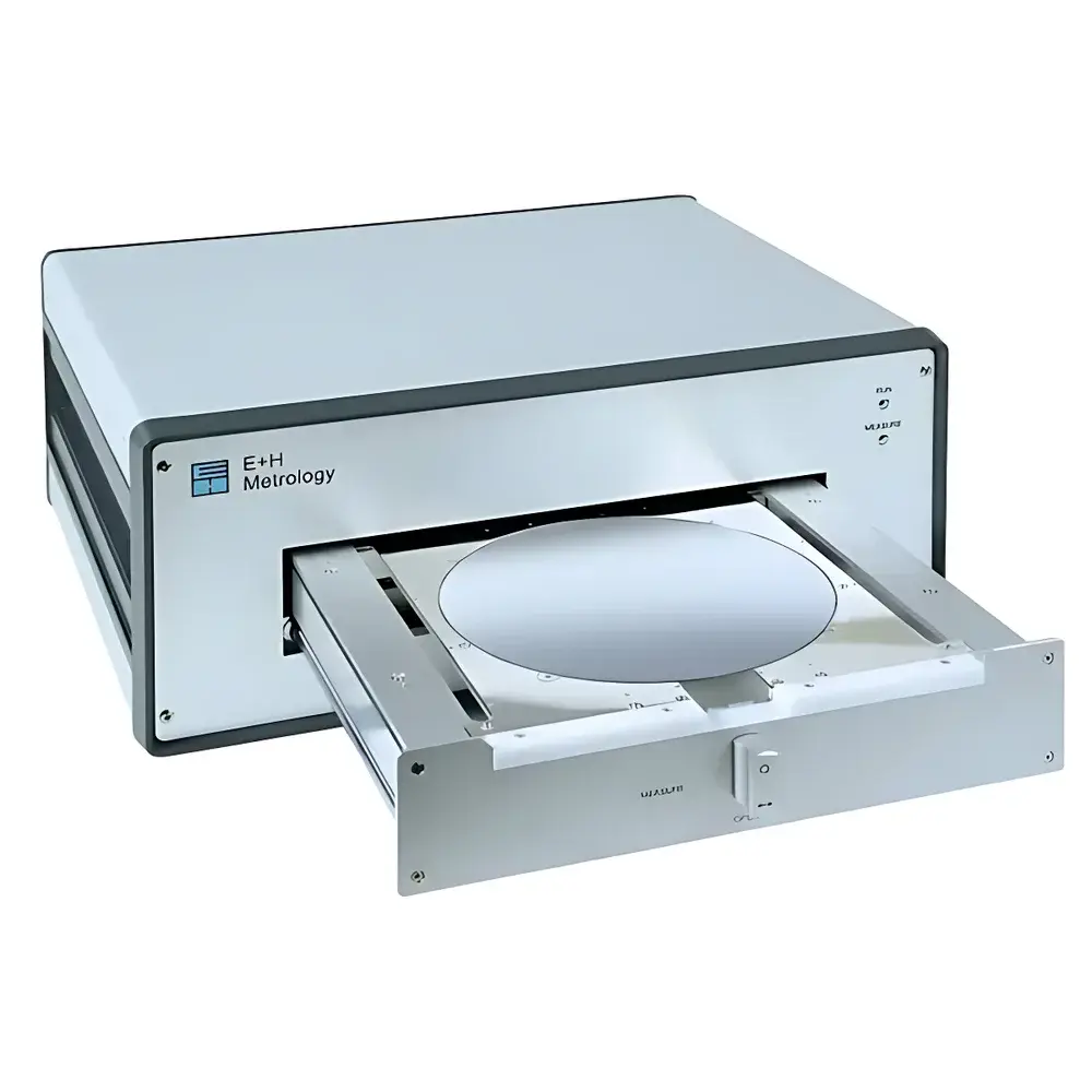
| Brand | Endress+Hauser Metrology |
|---|---|
| Country of Origin | Germany |
| Manufacturer Type | Authorized Distributor |
| Product Origin | Imported |
| Model | MX 203 |
| Pricing | Upon Request |
| Wafer Diameter Range | 50 mm – 450 mm (2″ – 18″) |
| Thickness Accuracy | ±0.5 µm |
| Thickness Resolution | 50 nm |
| Thickness Measurement Range | 100 µm – 1000 µm |
| Measurement Principle | Dual-Sided Capacitive Sensing |
| Automation Level | Manual Operation |
| Compatible Substrates | Si, SiC, GaN, GaAs, InP |
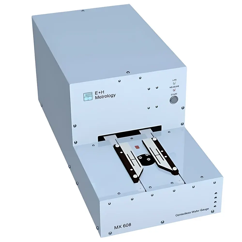
| Brand | Endress+Hauser Metrology |
|---|---|
| Origin | Germany |
| Model | MX608 |
| Wafer Diameter Support | 150 mm, 200 mm, 300 mm |
| Thickness Range | 500–800 µm |
| Max Warp | 100 µm |
| Resistivity Range | 0.001–200 Ω·cm |
| Thickness Accuracy | ±0.3 µm |
| TTV Accuracy | ±0.1 µm |
| Thickness Repeatability | ±0.05 µm |
| Resistivity Accuracy | ±1% (0.001–80 Ω·cm), ±5% (200 Ω·cm) |
| Resistivity Repeatability | ±0.2% (0.001–80 Ω·cm), ±2% (200 Ω·cm) |
| Edge Measurement Capability | up to 130 mm (150 mm wafers), up to 180 mm (200 mm wafers) |
| Single-Point Measurement Time | ~7 s |
| Full-Surface Scan (130/180 points) | ~10 s |
| Multi-Angle Radial Scan (18 scans @ 10° intervals) | ~3 min |
| Carrier Type Detection | P/N identification via Surface Photovoltage (SPV) |
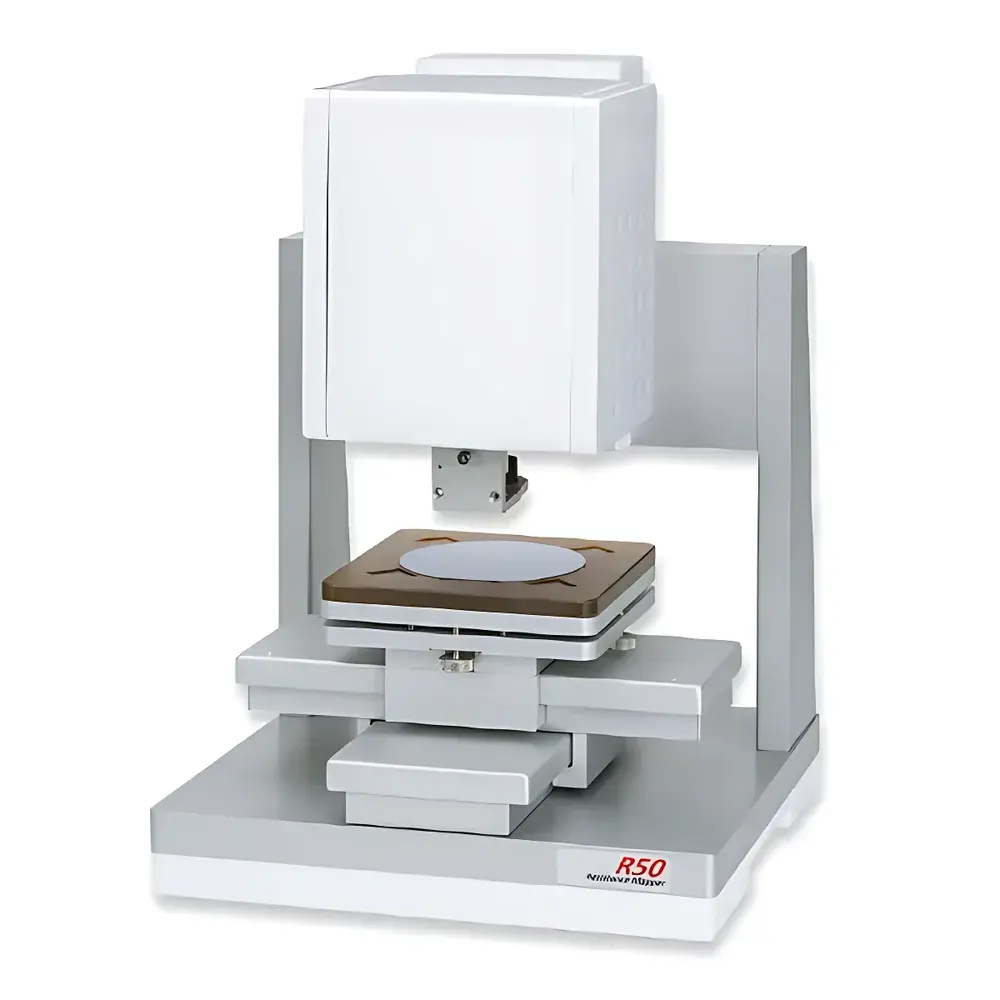
| Brand | Filmetrics |
|---|---|
| Origin | USA |
| Model | R50 |
| Measurement Principle | Contact Four-Point Probe (4PP) & Non-Contact Eddy Current (EC) |
| Max Sample Diameter | 300 mm |
| Max Mapping Area | 200 mm × 200 mm |
| XY Stage Travel Options | 100 mm × 100 mm or 200 mm × 200 mm (R50-200) |
| Z-Travel | 100 mm |
| Tilt Stage Range | ±5° |
| Mapping Speed | Up to 1 point/sec |
| Software | RsMapper™ with Pattern Generator, GLP-Compliant Data Logging |
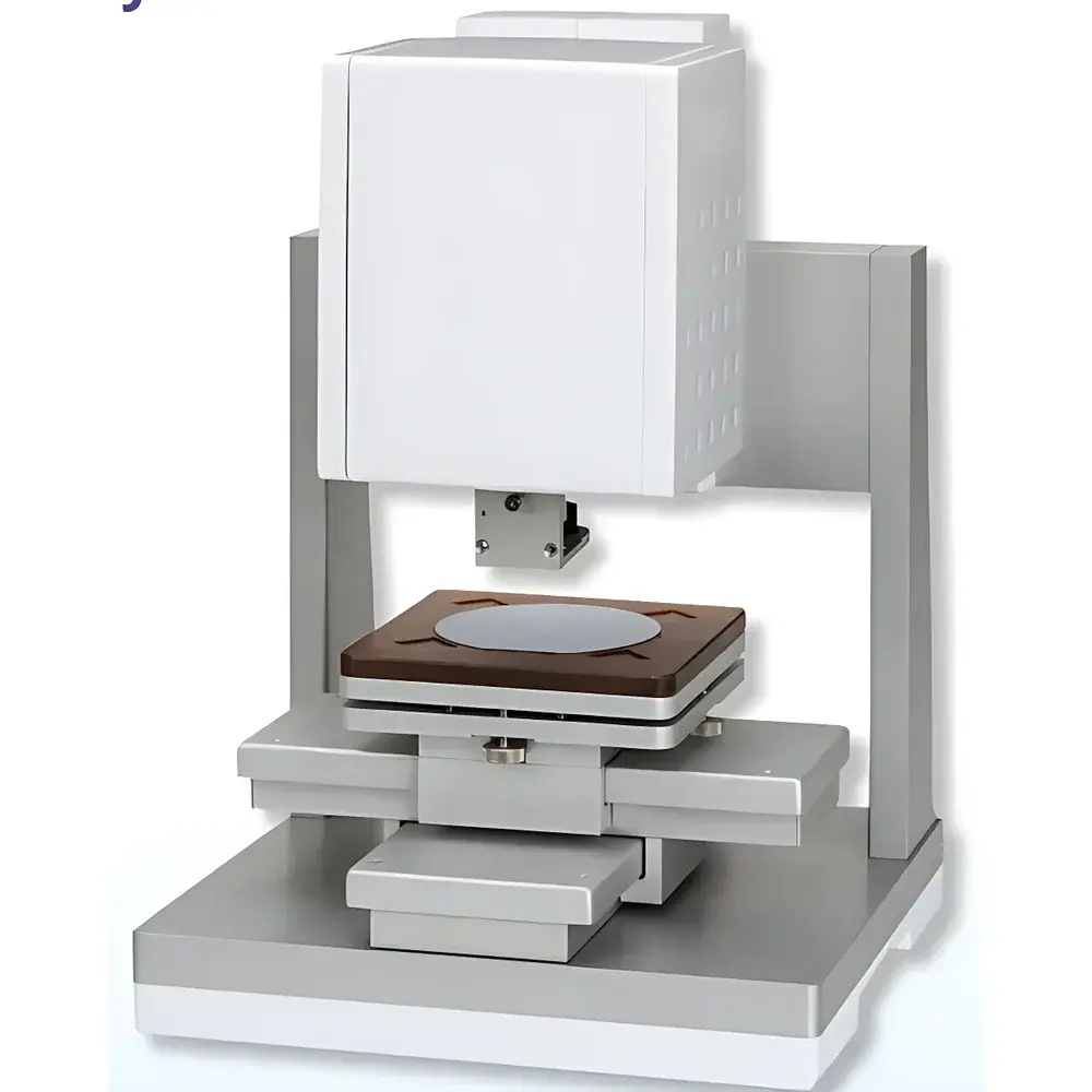
| Brand | KLA |
|---|---|
| Origin | USA |
| Manufacturer Type | Authorized Distributor |
| Product Origin | Imported |
| Model | Filmetrics R50 |
| Automation Level | Manual |
| Sheet Resistance Range | 1 mΩ/□ – 200 MΩ/□ |
| Sheet Resistance Accuracy | ±1% |
| Substrate Size Compatibility | 4-inch to 12-inch wafers |
| Software | RSMapper™ |
| Probe Compatibility | Fully compatible with KLA’s full suite of four-point probe sensors |
| XY Stage | 200 mm motorized |
| Z-Travel | 100 mm precision-controlled |
| Measurement Configurations | Customizable grid, linear, radial, and user-defined point patterns |
| Application Scope | Conductive & semiconducting thin films on Si, GaAs, SiC, sapphire, glass, and flexible substrates |
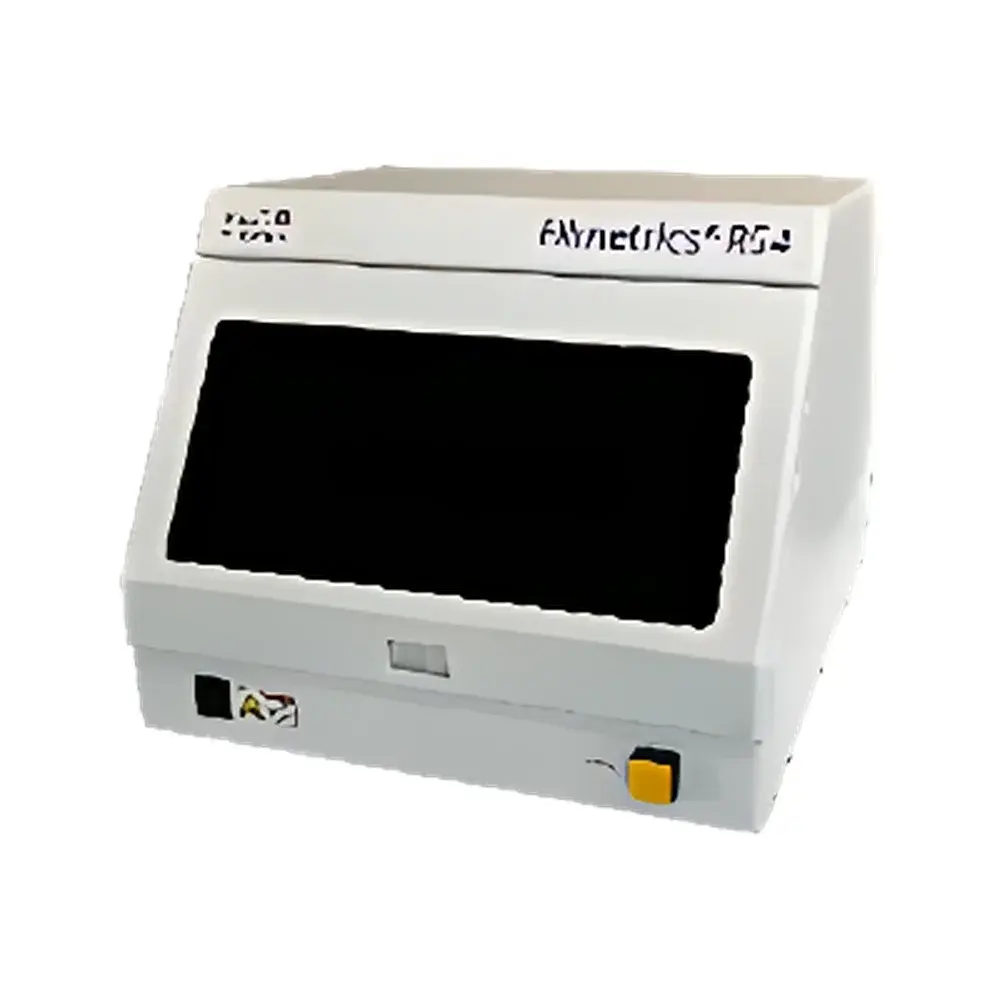
| Brand | KLA |
|---|---|
| Origin | USA |
| Manufacturer | KLA Corporation |
| Product Type | Imported Semiconductor Process Metrology Instrument |
| Automation Level | Fully Automated |
| Probe Configurations | Four-Point Probe (4PP) and Eddy Current (EC) |
| Maximum Sample Diameter | 200 mm (R54-200) or 300 mm (R54-300) |
| Maximum Sample Height | 15 mm |
| Sheet Resistance Range | 10⁻² to 10⁸ Ω/sq |
| Measurement Coordinate Modes | Rectangular, Linear, Polar, Custom Grid |
| XY Stage Precision | High-resolution motorized stage with ±100 mm travel (200 mm total range) |
| Enclosed Chamber | Yes, for light- and environment-sensitive samples |
| Software Platform | RSMapper™ v5.x with GLP-compliant audit trail, 21 CFR Part 11 optional modules |
| Compliance | ASTM F84, ISO 10777, SEMI MF67, USP <1054>, supports GMP/GLP documentation workflows |