Moji-Nano DLW-RD Desktop Economical 3D Laser Direct-Write System
| Brand | Moji-Nano |
|---|---|
| Origin | Shandong, China |
| Manufacturer Type | Original Equipment Manufacturer (OEM) |
| Country of Origin | China |
| Model | DLW-RD |
| Pricing | Upon Request |
Overview
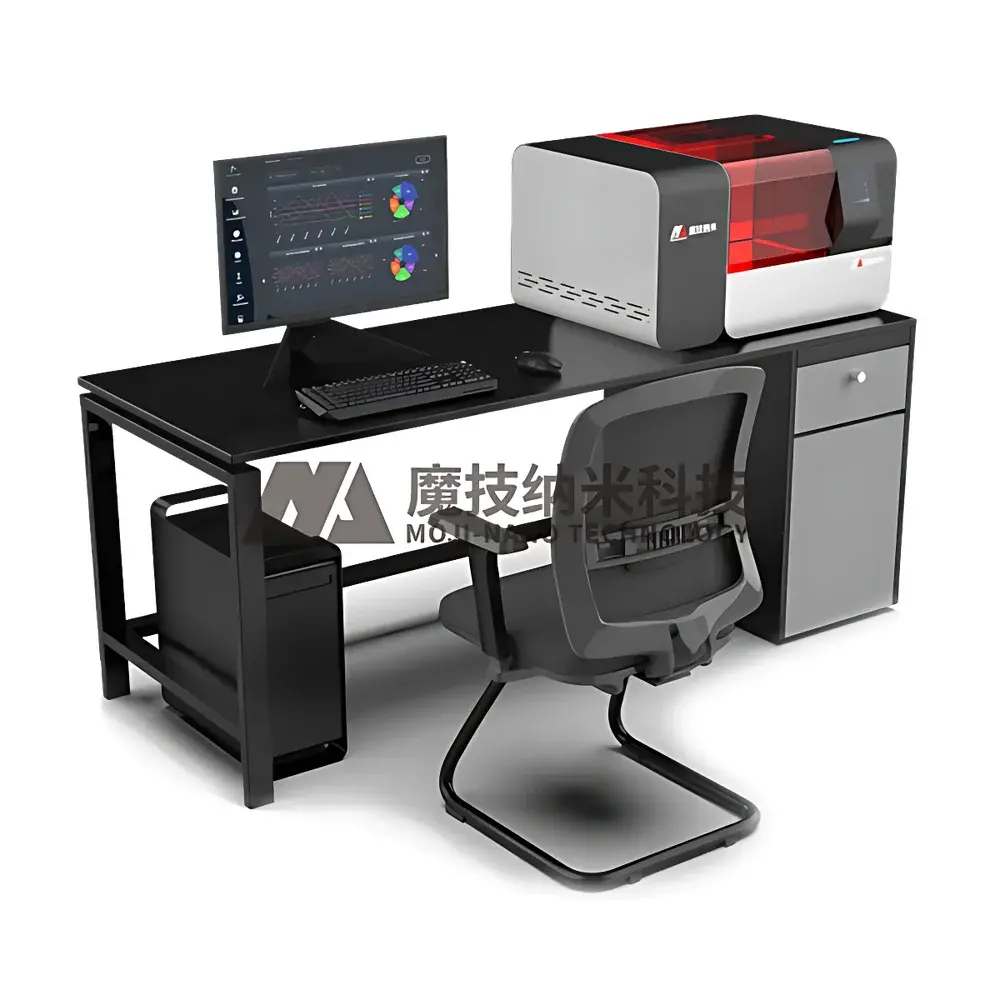
The Moji-Nano DLW-RD is a compact, desktop-class 3D laser direct-write system engineered for high-resolution micro- and nanoscale fabrication via multiphoton polymerization (MPP). Unlike conventional stereolithography (SLA) or digital light processing (DLP) systems, the DLW-RD employs tightly focused femtosecond near-infrared (NIR) laser pulses to induce nonlinear two-photon absorption within photosensitive resins—enabling true 3D voxel-by-voxel writing with sub-diffraction-limit spatial resolution. Its fully enclosed optical path minimizes environmental perturbations, while an integrated active vibration isolation platform and precision temperature stabilization subsystem ensure thermal and mechanical stability over extended write durations (>8 hours), critical for reproducible nanofabrication. Designed specifically for academic labs, R&D centers, and pilot-scale prototyping facilities, the DLW-RD bridges the gap between research-grade performance and cost-effective accessibility—delivering 70 nm feature resolution without requiring cleanroom infrastructure or ultra-high-power laser sources.
Key Features
- Multiphoton polymerization engine using ultrafast NIR laser (typically 780–800 nm, <150 fs pulse width) for true 3D submicron structuring
- Optically sealed beam path with anti-vibration optical table integration and closed-loop temperature control (±0.1 °C stability)
- High-precision galvanometric scanning stage combined with motorized Z-axis for dynamic focus tracking and layerless volumetric writing
- Modular resin compatibility—supports commercially available photoresists (e.g., IP-L, SZ2080, ORMOCER® derivatives) as well as custom-developed formulations
- Compact footprint (<0.8 m²) suitable for standard laboratory benches; CE-compliant electrical architecture and Class 1 laser safety enclosure
- Fully programmable scan parameters: laser power (0.1–50 mW at sample plane), scanning speed (1–500 µm/s), voxel dwell time (0.1–10 ms), and adaptive dose modulation
Sample Compatibility & Compliance
The DLW-RD accommodates substrates up to 100 mm × 100 mm × 20 mm (L×W×H), including silicon wafers, glass slides, ITO-coated substrates, flexible polymer films, and biocompatible hydrogel precursors. It supports both spin-coated and drop-cast resist layers (thickness range: 1–100 µm). All system hardware and firmware comply with IEC 60825-1:2014 (laser safety), IEC 61000-6-3:2019 (EMC emissions), and ISO 14001:2015 (environmental management). The control software architecture is designed to support audit trails and user access levels in accordance with GLP and ISO/IEC 17025 requirements, enabling traceability for regulated applications in biomedical device prototyping and micro-optics qualification.
Software & Data Management
Operation is managed through Moji-Nano’s proprietary NanoWrite Suite—a cross-platform application built on Qt/C++ with Python API extension support. The suite enables CAD-to-structure conversion (STL, OBJ, GDSII import), hierarchical structure definition, real-time power calibration, and automated batch job queuing. All process parameters, laser logs, environmental sensor data (temperature, humidity, stage position), and image-based alignment metadata are stored in timestamped SQLite databases compliant with FAIR data principles. Export formats include TIFF (for SEM/FIB correlation), HDF5 (for computational modeling input), and standardized JSON schemas compatible with LIMS integration. Optional FDA 21 CFR Part 11 compliance modules provide electronic signature enforcement, role-based permissions, and immutable audit logs.
Applications
- Biomedical Engineering: Fabrication of patient-specific scaffolds with controlled pore architecture (2–50 µm), microfluidic organ-on-chip interfaces, and bioresorbable microneedle arrays
- Micro-Optics: Freeform microlens arrays, photonic crystal slabs, waveguide splitters, and metasurface unit cells with phase-gradient control
- Metamaterials & Plasmonics: 3D chiral meta-atoms, negative-index lattices, and plasmonic nanoantenna clusters requiring precise inter-element spacing & orientation
- Micro-Electro-Mechanical Systems (MEMS):strong> Functional microactuators, tunable resonators, and encapsulated fluidic valves with embedded channels and hinges
- Materials Science: Template-assisted growth substrates for CVD nanowires, gradient-index composites, and stimuli-responsive hydrogel architectures
FAQ
What is the minimum achievable feature size under standard operating conditions?
The DLW-RD achieves a lateral resolution of ≤70 nm and axial resolution of ≤150 nm when using optimized photoresists (e.g., IP-L 780) and calibrated laser parameters.
Does the system support multi-material printing in a single run?
No—the DLW-RD is a single-resin platform per print job; however, sequential printing with manual substrate exchange and re-alignment is supported via fiducial-based coordinate registration.
Is remote operation and monitoring possible?
Yes—NanoWrite Suite includes secure WebSocket-based remote access with live camera feed, real-time parameter telemetry, and emergency stop override via authenticated TLS 1.3 connection.
What maintenance intervals are recommended for long-term reliability?
Laser source alignment verification every 6 months; objective lens cleaning and calibration every 3 months; vibration isolation platform damping fluid replacement annually.
Can the system be integrated into automated lab workflows?
Yes—via RESTful API endpoints and Python SDK, the DLW-RD supports scheduling through common laboratory orchestration platforms (e.g., Opentrons Flex, LabArchives, or custom MES integrations).
Related Products


