SIG Series LED Chip and Small LED Source Near-Field Measurement System
| Origin | USA |
|---|---|
| Manufacturer Type | Authorized Distributor |
| Origin Category | Imported |
| Model | SIG Series |
| Pricing | Available Upon Request |
Overview
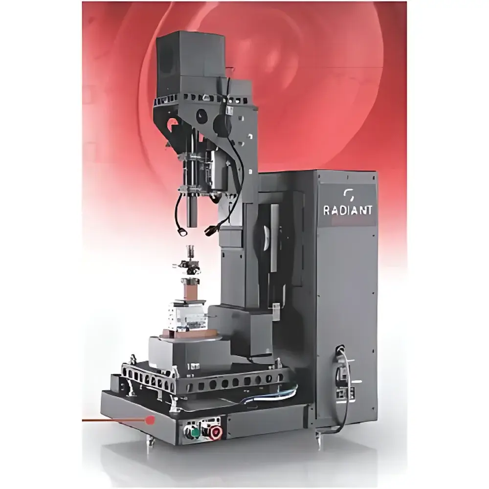
The SIG Series LED Chip and Small LED Source Near-Field Measurement System is a precision optical instrumentation platform engineered for high-fidelity spatial radiometric and photometric characterization of miniature light-emitting devices. Based on calibrated near-field goniophotometric acquisition, the system captures full 3D angular intensity distribution (Ray DATA) at sub-millimeter standoff distances—enabling deterministic reconstruction of far-field radiation patterns via rigorous weighted ray-tracing algorithms. Unlike conventional integrating sphere or far-field goniometer methods, this system preserves critical near-field phase and spatial coherence information essential for accurate chip-level optical modeling. It serves as a foundational metrology tool for R&D labs, LED packaging engineers, and optical designers requiring traceable, geometry-aware luminous intensity data compliant with CIE S 025/E:2015 and IES LM-79–19 measurement protocols.
Key Features
- Sub-50 µm spatial resolution near-field scanning over adjustable working distances (0.1–5 mm), optimized for bare die, COB, and 0402–3535 package formats
- Automated multi-axis positioning stage with ±0.05° angular repeatability and <0.1 µm linear step resolution
- Thermally stabilized silicon photodiode detector array with NIST-traceable spectral responsivity (380–780 nm, f1′ < 3.5%)
- Integrated thermal management subsystem maintaining DUT junction temperature within ±0.5°C during extended acquisition cycles
- Native export of industry-standard Ray DATA format (.rad, .ies, .ldt) with full metadata embedding (CCT, CRI, chromaticity coordinates, radiant flux)
- Hardware-synchronized trigger interface for pulsed LED testing (PWM dimming, transient response analysis)
Sample Compatibility & Compliance
The SIG Series accommodates a broad spectrum of solid-state emitters: bare GaN-based LED chips (100 × 100 µm to 1.5 × 1.5 mm), flip-chip configurations, micro-LED arrays, phosphor-converted white LEDs, and UV-A/UV-C miniature sources. All measurements adhere to ISO/CIE joint guidelines for near-field photometry, including strict control of ambient stray light (<0.01 lux), spectral irradiance uniformity (±1.2%), and geometric alignment tolerances per CIE 127:2007 Annex B. System calibration certificates are issued annually by an A2LA-accredited laboratory, supporting GLP-compliant documentation workflows and FDA 21 CFR Part 11 audit readiness when paired with optional secure logging modules.
Software & Data Management
Bundled SIG-Studio software provides a validated, Windows-based environment for acquisition control, real-time visualization, and model-driven far-field extrapolation. The software implements proprietary weighting kernels derived from Maxwell’s equations for non-paraxial propagation, achieving <±1.8% deviation from physical far-field validation at 1 m, 3 m, and 10 m distances. Export modules support direct one-click integration into Zemax OpticStudio (via .ZRD import), LightTools (native .LT format), and TracePro (compatible with .TRP and .RAD files). All datasets include embedded EXIF-style metadata tags—wavelength calibration date, aperture definition, integration time, and environmental sensor logs (temperature/humidity)—ensuring full traceability across design iteration cycles.
Applications
- LED packaging optimization: Quantifying sidewall emission, lens shadowing effects, and phosphor scattering anisotropy to guide mold design and conformal coating thickness
- Micro-LED display development: Characterizing pixel-level angular color shift (ACS) and luminance roll-off for HDR backlight and AR waveguide coupling simulations
- Luminaire optical engine validation: Generating physics-based source models that eliminate empirical “black box” approximations in lighting simulation
- DOE and TIR lens prototyping: Feeding measured near-field data directly into non-sequential ray tracing to accelerate tolerance stack-up analysis
- Photobiological safety assessment: Deriving spectral radiant intensity distributions required for IEC 62471 compliance testing of Class 1–3R LED products
FAQ
What distinguishes near-field measurement from traditional goniophotometry?
Near-field acquisition captures intensity and spectral data at distances comparable to the source’s physical dimensions—preserving spatial phase relationships lost in far-field averaging. This enables predictive modeling rather than empirical interpolation.
Can the system measure pulsed or modulated LEDs?
Yes—hardware-triggered synchronous acquisition supports PWM frequencies up to 10 MHz and transient pulse widths ≥100 ns, with time-resolved spectral binning capability.
Is calibration traceable to national standards?
All photometric and spectral calibrations are performed using NIST-traceable reference lamps and spectroradiometers, documented per ISO/IEC 17025 requirements.
Does the system support automated batch testing for production QA?
Optional scriptable automation mode (Python API) enables unattended measurement sequences with pass/fail thresholding against user-defined photometric limits.
How is thermal stability ensured during long-duration scans?
An integrated Peltier-controlled stage and real-time junction temperature feedback loop maintain thermal equilibrium within ±0.5°C—critical for reproducible luminous flux and CCT tracking.


