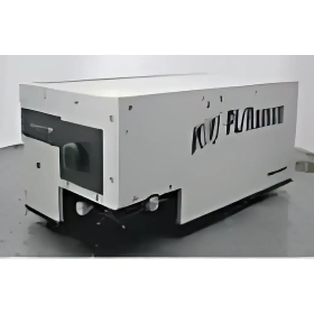
ZOLIX MiniPL 5.0 eV Deep-Ultraviolet Photoluminescence Mapping Spectrometer
| Brand | ZOLIX |
|---|---|
| Origin | Beijing, China |
| Manufacturer Type | Direct Manufacturer |
| Model | MiniPL 5.0 eV |
| Excitation Wavelengths | 224 nm (5.5 eV) or 248.6 nm (5.0 eV) |
| Spectral Range (Standard) | 190–650 nm |
| Spectral Range (Optional) | 190–850 nm |
| Resolution (Standard) | 0.2 nm @ 1200 g/mm grating |
| Resolution (Optional) | 0.07 nm @ 3600 g/mm grating |
| Detector | High-sensitivity PMT |
| Signal Processing | Built-in boxcar averager for pulsed signal integration |
| Sample Stage | Manual XYZ adjustment, max. 50 mm diameter |
| Optional | Motorized XY scanning stage for PL mapping |
| Dimensions | 15 × 18 × 36 cm |
| Weight | < 8 kg |
| Software Platform | LabVIEW-based control & spectral analysis suite |
Overview
The ZOLIX MiniPL 5.0 eV Deep-Ultraviolet Photoluminescence Mapping Spectrometer is a compact, modular, and computer-controlled photoluminescence (PL) characterization system engineered for high-sensitivity detection of broadband emission from wide-bandgap semiconductors. Operating on the principle of steady-state and time-gated photoluminescence spectroscopy, the instrument employs deep-ultraviolet (DUV) laser excitation—either at 224 nm (5.5 eV) or 248.6 nm (5.0 eV)—to efficiently populate valence-to-conduction band transitions in materials such as AlN, GaN, SiC, diamond, h-BN, and perovskite derivatives. Its optical architecture integrates optimized DUV-grade optics, a high-throughput Czerny–Turner monochromator, and a low-noise, side-on photomultiplier tube (PMT) detector with thermoelectric stabilization. The embedded boxcar averager enables precise time-domain gating synchronized to the pulsed laser source, significantly enhancing signal-to-noise ratio (SNR) for weak, nanosecond-scale PL decays—critical for quantitative defect-state analysis and quantum efficiency estimation.
Key Features
- Deep-UV excitation at 224 nm (5.5 eV) or 248.6 nm (5.0 eV), enabling resonant excitation of wide-bandgap materials (>3.1 eV) with minimal thermal background and surface recombination artifacts
- Standard spectral coverage from 190 nm to 650 nm; extendable to 850 nm via optional grating and detector configuration
- High optical resolution: 0.2 nm (with 1200 g/mm grating, standard) or 0.07 nm (with 3600 g/mm grating, optional), supporting fine-structure analysis of excitonic peaks and phonon replicas
- Integrated boxcar averager with variable gate width (10 ns–10 ms) and delay control, optimized for pulsed laser sources and lifetime-resolved PL measurements
- Compact footprint (15 × 18 × 36 cm) and lightweight design (< 8 kg), facilitating integration into gloveboxes, vacuum chambers, or cleanroom-compatible optical tables
- Manual XYZ sample stage accommodating up to 50 mm diameter substrates; precision micrometer-driven translation ensures repeatable positioning for point-spectrum acquisition
- Optional motorized XY scanning stage (±12.5 mm range, 1 µm step resolution) enables automated spatial mapping of PL intensity, peak wavelength, FWHM, and integrated area across wafer-scale samples
Sample Compatibility & Compliance
The MiniPL 5.0 eV is validated for use with bulk crystals, epitaxial wafers, thin films, powders, and nanostructured samples—including nitride-based LEDs, UV photodetectors, and quantum dot composites. Its DUV-compatible optical path avoids quartz absorption limitations below 200 nm, ensuring fidelity in near-band-edge emission quantification. The system supports ambient, inert-gas, and low-temperature (via external cryostat integration) measurement environments. From a regulatory standpoint, data acquisition and processing comply with GLP-aligned workflows: all spectra are timestamped, instrument parameters are logged automatically, and raw data files retain full metadata (excitation energy, integration time, grating position, PMT voltage). While not pre-certified for FDA 21 CFR Part 11, the LabVIEW-based software architecture permits implementation of user-defined audit trails, electronic signatures, and secure data archiving—meeting foundational requirements for GMP-compliant QC laboratories in semiconductor manufacturing.
Software & Data Management
Control and analysis are executed through a native LabVIEW application featuring intuitive graphical interface and scriptable automation (via VI scripting or Python API). Core functionalities include real-time spectrum preview, multi-curve overlay, peak search with Gaussian/Lorentzian fitting, FWHM and centroid wavelength calculation, spectral normalization (area or max-intensity), and derivative spectroscopy. For mapping applications, the software generates heatmaps of spectral parameters (e.g., peak shift vs. position) and exports georeferenced TIFF or HDF5 datasets compatible with MATLAB, Python (NumPy/SciPy), and industry-standard metrology platforms. All raw and processed data are saved in vendor-neutral formats (.txt, .csv, .xml) with embedded calibration coefficients, ensuring traceability and third-party reproducibility.
Applications
- Bandgap determination and strain analysis in AlGaN heterostructures via temperature-dependent PL peak tracking
- Quantitative assessment of Mg doping uniformity in p-type GaN layers using acceptor-bound exciton intensity ratios
- Defect-related deep-level emission mapping in SiC substrates to identify micropipe or stacking fault clusters
- In-line quality assurance of UV-LED epiwafers—measuring local variations in quantum well composition and crystalline quality
- Time-resolved PL decay profiling for carrier lifetime extraction in perovskite thin-film solar cells
- Complementary use with Raman spectroscopy (via shared DUV excitation path) for concurrent phonon and electronic structure characterization
FAQ
What excitation wavelengths does the MiniPL support, and why are they critical for wide-bandgap materials?
The system offers selectable 224 nm (5.5 eV) and 248.6 nm (5.0 eV) DUV laser lines. These energies exceed the bandgaps of AlN (~6.2 eV), GaN (~3.4 eV), and SiC (~3.3 eV), enabling direct interband excitation with minimized non-radiative surface contributions.
Can the MiniPL perform absolute quantum yield measurements?
Yes—the system supports relative and calibrated absolute photoluminescence quantum yield (PLQY) via integrating sphere coupling and reference standard protocols (e.g., using BaSO₄ or certified fluorescent standards), provided the optional sphere module is installed.
Is vacuum or purged operation required for measurements below 200 nm?
For optimal transmission below 190 nm, nitrogen purging or vacuum operation is recommended to mitigate O₂ and H₂O absorption; the optical path is designed for easy integration with standard purge manifolds.
How is spectral calibration maintained over time?
Wavelength calibration is performed using Hg/Ar spectral lamps (included), with polynomial fitting applied during startup; intensity calibration uses NIST-traceable tungsten halogen standards (optional accessory).
Does the system support synchronization with external equipment such as pulse generators or cryostats?
Yes—TTL trigger I/O ports enable hardware-level synchronization with laser drivers, temperature controllers, and motion stages, ensuring phase-coherent data acquisition in complex experimental configurations.

")

