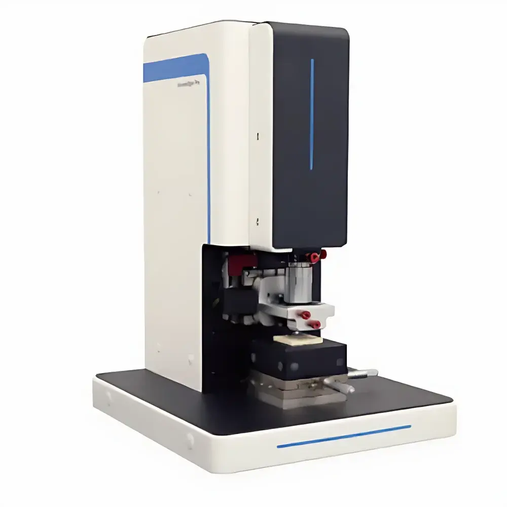
AtomEdge Pro Atomic Force Microscope by Truth Instruments
| Brand | Truth Instruments Company Limited |
|---|---|
| Origin | Beijing, China |
| Manufacturer Type | Authorized Distributor |
| Country of Origin | China |
| Model | AtomEdge Pro |
| Pricing | Available Upon Request |
Overview
The AtomEdge Pro Atomic Force Microscope (AFM) is a high-performance scanning probe microscope engineered for nanoscale surface characterization in research laboratories and industrial quality control environments. Operating on the principle of mechanical force detection via a sharp tip mounted on a microfabricated cantilever, the AtomEdge Pro measures interatomic forces—including van der Waals, capillary, electrostatic, and magnetic interactions—to generate topographic, mechanical, electrical, and magnetic property maps with sub-nanometer vertical resolution and lateral resolution down to ~0.5 nm under optimal conditions. Designed for versatility across ambient, liquid, and controlled-environment configurations, the system supports contact, tapping, non-contact, and advanced dynamic modes (e.g., PeakForce Tapping®, amplitude modulation, frequency modulation), enabling quantitative nanomechanical mapping (modulus, adhesion, deformation) and electrical characterization (KPFM, C-AFM, SSRM) without requiring ultra-high vacuum or conductive sample preparation.
Key Features
- Modular platform architecture with interchangeable scanner heads (100 × 100 × 15 µm and 30 × 30 × 15 µm piezoelectric scanners) optimized for speed, linearity, and low thermal drift
- Low-noise, high-bandwidth optical beam deflection (OBD) detection system with <10 pm RMS noise floor over 1 kHz bandwidth
- Integrated environmental control module supporting temperature-regulated sample stages (−20 °C to +80 °C) and optional acoustic/vibration isolation enclosures
- Real-time multi-channel data acquisition at up to 4 MHz sampling rate, synchronized with laser Doppler vibrometer and external stimulus sources (e.g., bias voltage, nanoindenter)
- Automated tip approach and intelligent scan parameter optimization powered by embedded AI-assisted feedback algorithms
- Compliant with ISO/IEC 17025 calibration traceability framework; all position sensors calibrated against NIST-traceable interferometric standards
Sample Compatibility & Compliance
The AtomEdge Pro accommodates a broad range of sample types—including conductive and insulating thin films, biological specimens (cells, proteins, DNA), polymers, 2D materials (graphene, TMDCs), ceramics, and semiconductor wafers—without mandatory metallization or vacuum compatibility constraints. Sample mounting is facilitated via standard 12 mm and 25 mm magnetic discs, custom holders for TEM grids or fluid cells, and vacuum-compatible sample stages for in situ electrochemical AFM (EC-AFM). The instrument meets electromagnetic compatibility requirements per IEC 61326-1:2013 and safety standards per IEC 61010-1:2010. Data integrity workflows align with GLP and GMP principles, supporting audit-ready metadata logging including operator ID, timestamp, environmental conditions, and calibration history.
Software & Data Management
Control and analysis are performed using the proprietary NanoScope Suite v5.2, a Windows-based application certified for FDA 21 CFR Part 11 compliance (electronic signatures, role-based access control, immutable audit trails). The software provides real-time FFT spectral analysis, automated grain boundary detection, cross-sectional roughness profiling (Ra, Rq, Rz per ISO 4287), and export to industry-standard formats (Gwyddion .gws, WSxM .sxm, HDF5, TIFF, CSV). Raw force-distance curves and time-series datasets are stored in vendor-neutral HDF5 containers with embedded metadata schemas compliant with the FAIR (Findable, Accessible, Interoperable, Reusable) data principles. Remote operation and monitoring are supported via secure TLS-encrypted API endpoints compatible with LabArchives ELN and MATLAB-based custom scripting.
Applications
- Nanomechanical property mapping of battery electrode coatings (Young’s modulus, creep behavior, SEI layer homogeneity)
- Topographic and phase imaging of lipid bilayers and membrane protein complexes under physiological buffer conditions
- Defect inspection and critical dimension metrology for EUV photomasks and advanced packaging substrates
- In situ observation of crystal nucleation and growth kinetics during solvent evaporation or electrochemical deposition
- Quantitative charge distribution analysis of ferroelectric domains using Kelvin Probe Force Microscopy (KPFM)
- Adhesion force quantification between functionalized AFM tips and biofunctionalized surfaces for biosensor development
FAQ
Is the AtomEdge Pro compatible with third-party probes and cantilevers?
Yes—it accepts standard 125 µm × 125 µm × 500 µm rectangular cantilevers from Bruker, Nanoworld, Olympus, and BudgetSensors, with automatic recognition of nominal spring constant and resonance frequency via integrated cantilever identification protocol.
Does the system support in situ electrical biasing during scanning?
Yes—the integrated 10 V/100 mA bipotentiostat module enables simultaneous topography and current mapping (C-AFM) with sub-picoampere sensitivity and programmable ramp/step waveforms.
What level of training and technical support is provided upon installation?
Truth Instruments delivers a 3-day on-site commissioning and operator certification program, followed by quarterly remote performance validation and lifetime access to the NanoScope Knowledge Base and live engineering support (response SLA: ≤4 business hours for critical issues).


