Atometrics AF-3000 Series T001 Spectral Reflectometry Thin-Film Thickness Metrology System
| Brand | Atometrics |
|---|---|
| Origin | Guangdong, China |
| Manufacturer Type | Original Equipment Manufacturer (OEM) |
| Regional Classification | Domestic (China) |
| Model | AF-3000 Series T001 |
| Pricing | Upon Request |
Overview
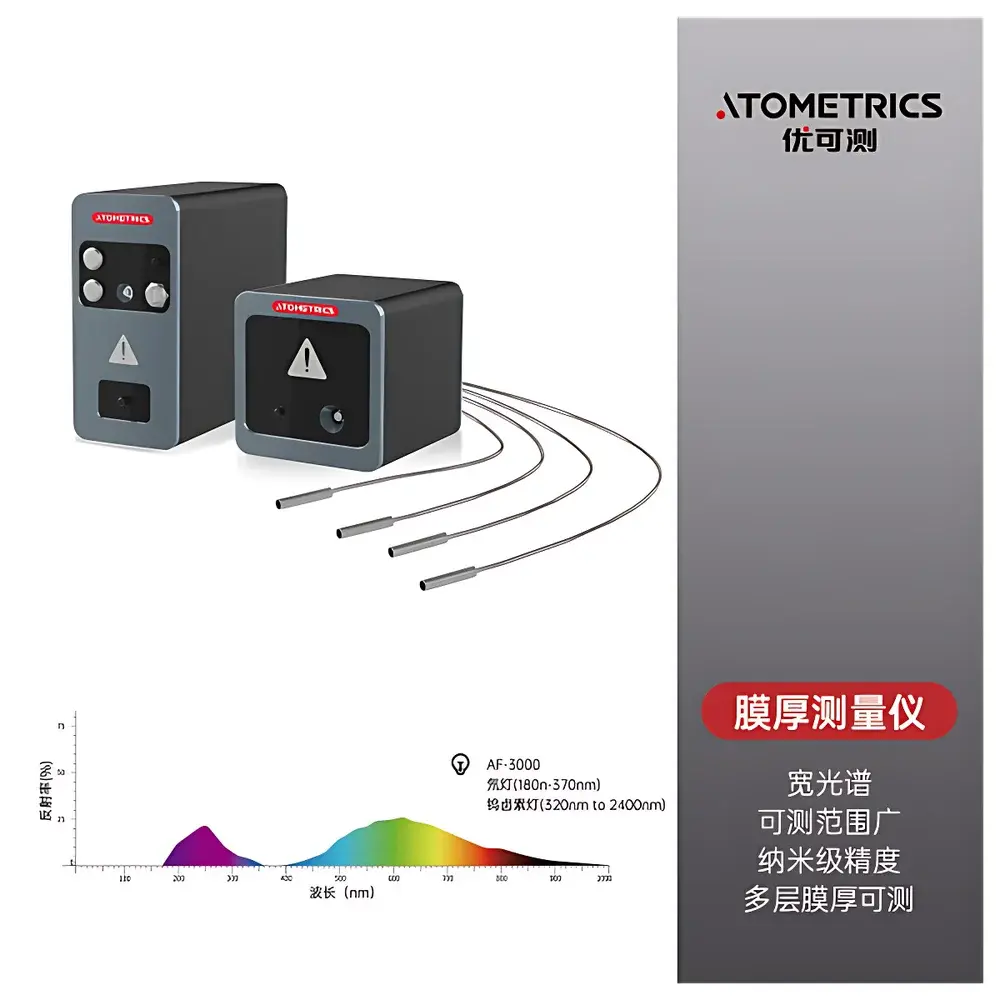
The Atometrics AF-3000 Series T001 is a high-precision spectral reflectometry-based thin-film thickness metrology system engineered for non-contact, non-destructive measurement of single-layer and multilayer thin films across R&D, process development, and production environments. Operating on the physical principle of broadband optical interference—where incident light reflects at interfaces between layers with differing refractive indices—the system reconstructs film thickness and optical constants (n, k) by fitting measured reflectance spectra against theoretical models using a proprietary segmented spectral fitting algorithm. Unlike conventional instruments relying on global curve fitting over the full spectrum, the AF-3000’s segmented approach partitions the spectral domain (e.g., UV: 180–370 nm; Vis-NIR: 320–2400 nm) and applies independent optimization per band, significantly reducing systematic deviation caused by dispersion model inaccuracies or source intensity non-uniformity. This architecture enables sub-angstrom resolution in thickness determination—verified under controlled calibration conditions—and supports measurement of complex stacks including liquid films, air gaps, rough interfaces, and transparent/absorbing layers.
Key Features
- Segmented spectral fitting algorithm: Minimizes fitting error by optimizing optical constants and thickness independently within UV (deuterium lamp, 180–370 nm) and Vis-NIR (tungsten-halogen lamp, 320–2400 nm) bands
- High-intensity, spectrally stable illumination: Dual-source configuration ensures uniform photon flux and low noise across the entire operational range
- Multi-mode deployment flexibility: Supports offline benchtop, inline process monitoring (sampling interval < 100 ms), and fully automated wafer-handling configurations
- Extended layer capacity: Capable of modeling and quantifying up to 10 discrete layers in a single stack, including semi-transparent, absorbing, and graded-index films
- Sub-angstrom thickness resolution: Achieved through high signal-to-noise ratio detection and advanced dispersion modeling—validated via NIST-traceable reference standards
- Compact optical head design: Enables integration into cleanroom tools, vacuum chambers, or confined manufacturing spaces without compromising optical path integrity
Sample Compatibility & Compliance
The AF-3000 Series T001 accommodates a broad range of substrate and film types—including silicon wafers (4”, 6”, 8”, and 12”), glass substrates, flexible polymer films (e.g., PI, PET), and microfluidic devices—with minimal sample preparation. It measures thicknesses from ~1 nm (e.g., ITO monolayers, perovskite seed layers) up to >30 µm (e.g., photoresist, thick dielectrics), with demonstrated performance across industry-relevant materials such as SiO₂, quantum dots, metal oxides, and organic semiconductors. The system complies with ISO/IEC 17025 requirements for calibration traceability and supports audit-ready data logging aligned with GLP and GMP documentation frameworks. While not certified to FDA 21 CFR Part 11 out-of-the-box, its software architecture permits configuration for electronic signature, audit trail, and role-based access control—enabling validation for regulated pharmaceutical or medical device manufacturing environments.
Software & Data Management
The AF-3000 is operated via Atometrics’ proprietary MetroSuite™ software, a Windows-based platform supporting real-time spectral acquisition, multi-layer optical modeling (Cauchy, Sellmeier, Tauc-Lorentz dispersion functions), and batch analysis workflows. All raw spectra, fit parameters, residuals, and uncertainty estimates are stored in HDF5 format—ensuring long-term readability and interoperability with Python, MATLAB, and LabVIEW. The software includes built-in statistical process control (SPC) modules, cross-platform report generation (PDF/CSV/XLSX), and API-level integration via TCP/IP or USB virtual COM port for factory automation (SECS/GEM compatibility available upon request). Full version control, user activity logs, and encrypted database storage meet baseline requirements for ISO 9001 and IATF 16949 quality management systems.
Applications
- Photovoltaics: Thickness and composition profiling of perovskite absorber layers, HTL/ETL stacks, and anti-reflection coatings
- Semiconductor fabrication: In-line monitoring of PECVD SiNₓ, ALD Al₂O₃, and spin-on dielectrics during wafer processing
- Display technology: Characterization of ITO, Ag nanowire, and QD color filter films on rigid and flexible substrates
- MEMS & microfluidics: Quantification of channel depth, bonding interface integrity, and PDMS/SiO₂ layer uniformity
- Advanced packaging: Measurement of under-bump metallization (UBM) stacks and redistribution layer (RDL) thickness variation
- R&D laboratories: Rapid optical constant extraction for novel 2D materials (e.g., MoS₂, h-BN) and hybrid organic-inorganic films
FAQ
What is the minimum measurable thickness for ultra-thin films such as monolayer graphene or native oxide?
The AF-3000 Series T001 achieves reliable detection down to approximately 0.5 nm for optically distinct layers on reflective substrates (e.g., Si wafers), contingent upon sufficient contrast in refractive index and surface roughness below 0.3 nm RMS.
Does the system support real-time feedback for closed-loop process control?
Yes—via configurable digital I/O and Ethernet-based command protocol, the AF-3000 can deliver thickness values at ≤100 ms intervals to PLCs or host MES systems for adaptive endpoint detection.
Can it measure films on curved or textured surfaces?
The instrument supports limited curvature (radius ≥ 50 mm) and moderate surface roughness (Ra < 5 nm); for highly structured or microlens arrays, spot size reduction and tilt compensation options are available.
Is spectral calibration traceable to national standards?
All factory calibrations are performed using NIST-traceable reference standards (SRM 2036, SRM 1020), with certificate of calibration provided per unit shipment.
How is measurement repeatability validated across different operators and environmental conditions?
The system includes integrated drift compensation routines, temperature-stabilized optics, and standardized SOP templates compliant with ASTM E2914 and ISO 15504 for metrological verification.


