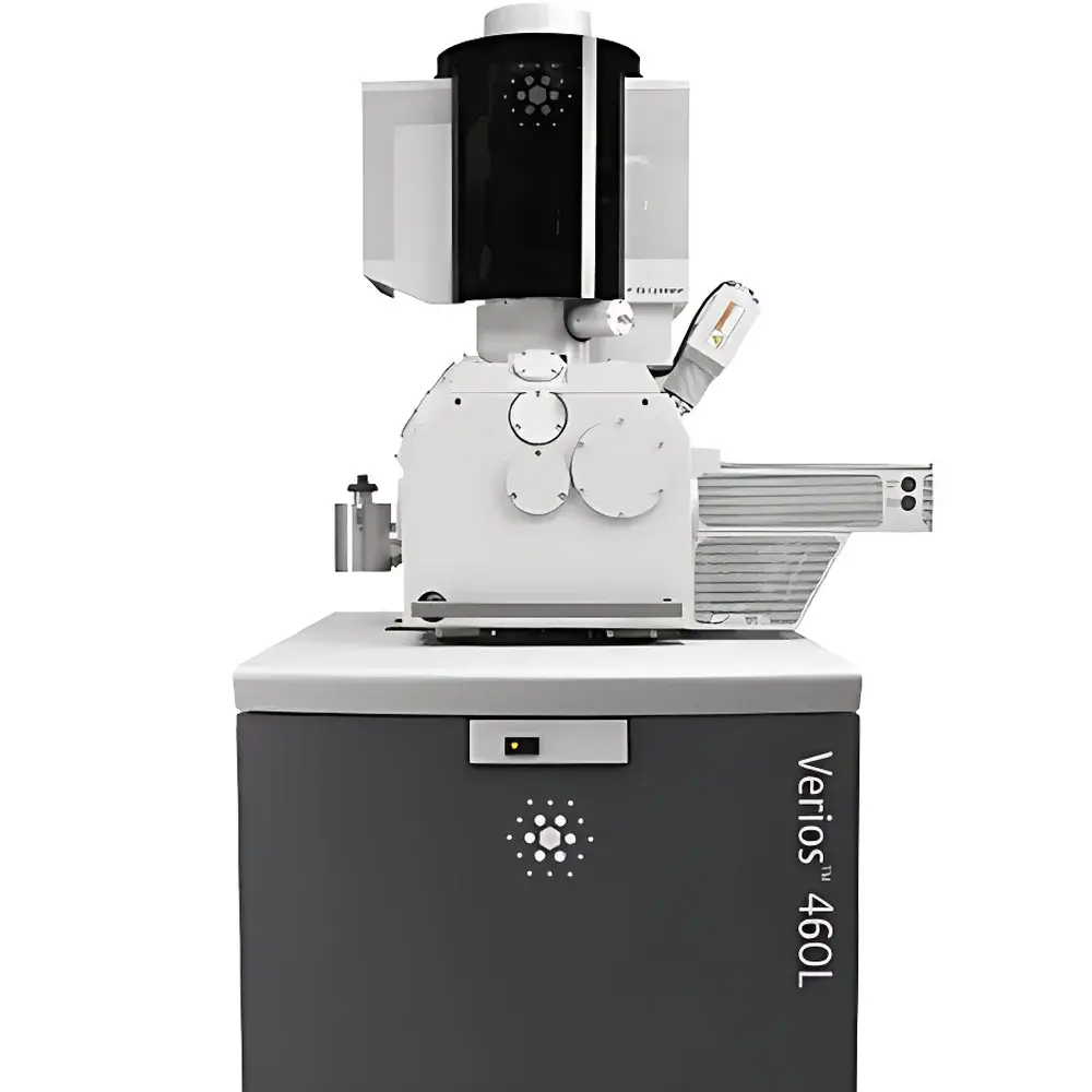
Thermo Fisher Scientific Verios XHR Scanning Electron Microscope
| Brand | Thermo Fisher Scientific |
|---|---|
| Origin | Czech Republic |
| Manufacturer Type | Original Equipment Manufacturer (OEM) |
| Origin Category | Imported |
| Model | Verios XHR |
| Instrument Type | Floor-standing / Conventional High-Performance SEM |
| Electron Source | Cold Field Emission Gun (CFEG) |
| Accelerating Voltage Range | 1–30 kV |
| Secondary Electron Resolution | <0.7 nm at 1 kV, <0.4 nm at 30 kV (as specified in Thermo Fisher technical documentation) |
| Backscattered Electron Resolution | <1.5 nm at 30 kV |
| Sample Chamber Dimensions | Ø340 mm × H280 mm |
| Maximum Sample Size | 200 mm wafer or 100 mm × 100 mm × 50 mm bulk specimen |
Overview
The Thermo Fisher Scientific Verios XHR Scanning Electron Microscope (SEM) represents the second-generation evolution of FEI’s flagship XHR (eXtreme High Resolution) platform. Engineered for precision nanoscale characterization across semiconductor metrology, advanced materials research, and life sciences, the Verios XHR leverages cold field emission electron optics combined with electrostatic beam deceleration and high-efficiency signal detection to deliver sub-nanometer resolution across a broad accelerating voltage range (1–30 kV). Unlike conventional thermionic or Schottky-emission SEMs, its CFEG source provides exceptional brightness, energy spread <0.3 eV, and long-term current stability—enabling consistent high-resolution imaging and quantitative analysis without beam-induced drift or thermal instability. The system operates on the fundamental principle of raster-scanned electron-sample interaction, where incident electrons generate secondary electrons (SE), backscattered electrons (BSE), and characteristic X-rays; these signals are spatially resolved by synchronized scanning and digitized for topographic, compositional, and crystallographic interpretation.
Key Features
- Cold Field Emission Gun (CFEG) with ultra-low energy spread (1 × 10⁹ A/cm²·sr·V), ensuring stable probe current and minimal chromatic aberration
- Electrostatic Beam Deceleration (EBD) technology enabling high-resolution imaging at low landing energies (down to 1 kV) while preserving signal-to-noise ratio and surface sensitivity
- Through-the-lens detector (TLD) optimized for secondary electron collection with enhanced contrast for insulating and beam-sensitive specimens
- Dedicated low-voltage BSE detector with annular geometry for simultaneous material-contrast mapping at sub-5 kV conditions
- Beam blanking and dose control system for precise electron dose management—critical for cryo-SEM, polymer, and biological applications
- Electrostatic scanning optics minimizing image distortion and scan lag, supporting high-speed acquisition up to 60 fps at 1024 × 768 pixels
- Large-volume chamber (Ø340 mm × H280 mm) accommodating full 200 mm wafers, cross-sectioned devices, or metallurgical mounts without repositioning
Sample Compatibility & Compliance
The Verios XHR supports diverse sample types—from conductive silicon wafers and TEM lamellae to non-conductive catalyst nanoparticles, hydrated cryo-sections, and unstained biological tissues. Its low-kV capability (1–5 kV) mitigates charging artifacts on insulators and reduces radiation damage in organic and soft matter systems. For regulated environments, the platform is compatible with GLP/GMP workflows through optional audit-trail-enabled software modules compliant with FDA 21 CFR Part 11. All vacuum subsystems meet ISO 27427 (electron microscope vacuum requirements), and stage motion repeatability adheres to ASTM E1558 standards for dimensional metrology. Optional cryo-transfer and in-situ heating stages extend operational compliance to ISO/IEC 17025-accredited laboratories performing nanoscale failure analysis.
Software & Data Management
Acquisition and analysis are managed via Thermo Fisher’s AutoScript 4 platform—a Python-based scripting environment supporting automated workflows, batch imaging, and metrology routines (e.g., line width, edge roughness, particle size distribution). Image data is stored in standardized TIFF + metadata format, with embedded calibration, acquisition parameters, and user annotations. Integration with Thermo Fisher’s Connect software enables centralized instrument monitoring, remote diagnostics, and secure cloud-based data sharing across multi-site R&D teams. All software modules support role-based access control and electronic signature functionality required for regulated quality assurance processes.
Applications
- Semiconductor Process Control: Critical dimension (CD) metrology of FinFETs, GAA transistors, and EUV lithography patterns at 22 nm node and below; defect review of mask blanks and etched wafers
- Materials Science: In-situ observation of nanoparticle sintering, grain boundary dynamics, phase segregation in battery cathodes, and pore network quantification in MOFs and aerogels
- Life Sciences: High-fidelity imaging of freeze-fractured membranes, immunogold-labeled organelles, and unstained extracellular vesicles—without metal coating or dehydration
- Geosciences & Catalysis: Surface texture analysis of shale matrix porosity, catalyst support morphology, and reaction-induced surface reconstruction under variable pressure conditions
- Failure Analysis: Cross-sectional imaging of solder joint voids, delamination in stacked-die packages, and electromigration-induced voiding in Cu interconnects
FAQ
What is the minimum landing voltage supported for high-resolution imaging?
The Verios XHR achieves <0.7 nm secondary electron resolution at 1 kV using electrostatic beam deceleration and optimized signal detection.
Can the system accommodate full 300 mm wafers?
No—the maximum supported wafer diameter is 200 mm; larger substrates require sectioning or use of alternative platforms such as the Thermo Fisher Helios Hydra.
Is EDS elemental mapping supported natively?
Yes—when equipped with an optional silicon drift detector (SDD), the Verios XHR supports real-time EDS mapping with spatial resolution down to 5 nm at 15 kV.
Does the system support automated particle analysis?
Yes—AutoScript 4 includes validated templates for ISO 13322-2 compliant particle sizing, shape classification, and agglomerate dispersion analysis.
What vacuum level is maintained in the gun chamber during operation?
The CFEG column operates at ≤2 × 10⁻¹⁰ mbar, ensuring >6-month emitter lifetime and minimal contamination-induced resolution loss.


