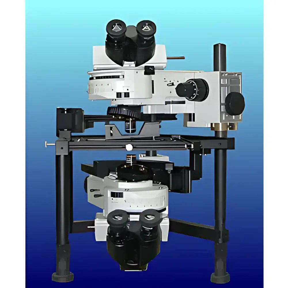
Nanonics MV2000 NSOM/SNOM-AFM Hybrid Scanning Probe Microscope
| Brand | Nanonics |
|---|---|
| Origin | Israel |
| Manufacturer Type | OEM Manufacturer |
| Origin Category | Imported |
| Model | MV2000 |
| Instrument Type | Materials-Focused Hybrid SPM Platform |
| Positional Detection Noise | 0.2 nm (RMS) |
| Maximum Sample Size | 6 mm (standard) |
| Sample Stage Scan Range | 80 µm × 80 µm × 80 µm (XYZ) |
| Z-Direction Resolution | < 0.05 nm (RMS) |
| XY Lateral Resolution (AFM) | < 0.15 nm |
| Near-Field Optical Resolution | ≤ 50 nm (aperture-limited) |
| Far-Field Optical Resolution | ~500 nm (non-confocal), ~200 nm (confocal) |
| Thermal Imaging Resolution | ≥ 100 nm |
| Electrical Resistance Mapping Resolution | ≥ 25 nm |
| Operating Temperature Range (Thermal Probes) | Up to 300 °C |
| Feedback Mechanism | Tuning Fork (standard), Laser Reflectance (optional) |
| Probe Compatibility | Glass fiber NSOM probes (patented bent-cantilever design), commercial Si/SiN AFM probes, custom multi-functional probes (optical/thermal/electrical/Raman-enhancing) |
Overview
The Nanonics MV2000 is a fully integrated, research-grade near-field scanning optical microscope (NSOM/SNOM) and atomic force microscope (AFM) hybrid platform engineered for quantitative nanoscale correlative characterization. Unlike conventional standalone SPM or optical systems, the MV2000 implements a true dual-scanning architecture—featuring independent, co-aligned sample and probe positioning stages—enabling simultaneous, non-interfering operation of far-field optics, near-field illumination/collection, mechanical force mapping, thermal conductivity profiling, and electrical resistance imaging. Its core measurement principle relies on evanescent field coupling via sub-diffraction-limit apertured optical probes (typically metal-coated tapered glass fibers with ≤ 50 nm apertures), where localized light–matter interaction occurs within the near-field zone (< λ/10). This enables spatial resolution decoupled from visible-light diffraction limits while maintaining compatibility with standard optical detectors (PMT, APD, InGaAs, CCD) and spectrometers. The system operates across UV–NIR spectral ranges and supports vacuum, ambient, and liquid environments—making it suitable for materials science, semiconductor metrology, photonic device analysis, and soft-matter biophysics.
Key Features
- Patented 3D Planar Scanning Architecture: Dual-stage design with independent 80 µm XYZ sample stage and 30 µm XYZ probe stage, enabling full optical access from both top and bottom without hardware reconfiguration.
- Tuning Fork-Based Force Feedback: Mechanically robust, low-noise detection ideal for NSOM–AFM–Raman concurrent operation—eliminates laser interference issues common in optical-lever AFM in optical microscopy configurations.
- Optically Transparent Glass Fiber Probes: Proprietary bent-cantilever geometry ensures high-efficiency waveguide transmission, polarization preservation, and compatibility with illumination-collection, collection-only, reflection, and transmission NSOM modalities.
- Multi-Functional Probe Integration: Supports simultaneous deployment of up to four independently controlled probes—including NSOM, thermal (dual Pt nanowire), conductive, and TERS-optimized gold-sphere-tipped probes—for parallel nanomechanical, nanothermal, nano-electrical, and nanooptical measurements.
- Deep-Trench Imaging Capability: Z-range up to 140 µm (MV4000 variant) with specialized cantilevers enables sidewall and bottom-of-trench topography and optical characterization of high-aspect-ratio structures.
- Open Modular Platform: Designed for seamless integration with commercial Raman spectrometers (e.g., Renishaw, Horiba), SEM/FIB columns, confocal microscopes, and cryogenic stages—fully compliant with ISO/IEC 17025 laboratory infrastructure requirements.
Sample Compatibility & Compliance
The MV2000 accommodates samples ranging from standard 6 mm wafers to custom substrates up to 200 mm in diameter, including cross-sectioned devices, rough surfaces, and heterogeneous multilayer stacks. Its open optical path supports both upright and inverted microscope configurations, enabling transmission-mode NSOM on transparent substrates (e.g., ITO/glass) and reflection-mode on opaque films (e.g., SiN, metals, OLED stacks). All operational modes—including contact, tapping, and non-contact AFM; aperture-based NSOM; tip-enhanced Raman spectroscopy (TERS); and nanothermometry—are validated per ASTM E2539 (SPM terminology), ISO/IEC 17025 (testing laboratory competence), and aligned with FDA 21 CFR Part 11 requirements for electronic records when paired with Nanonics’ audit-trail-enabled acquisition software. System calibration protocols follow NIST-traceable standards for dimensional, thermal, and optical performance verification.
Software & Data Management
Acquisition and analysis are performed using Nanonics’ proprietary NanoNavigator™ software suite, built on a modular, Python-extendable architecture. It provides synchronized multi-channel data capture (topography, optical intensity, phase, current, temperature gradient, Raman shift) with real-time cross-correlation visualization. All raw datasets are stored in HDF5 format with embedded metadata (timestamp, instrument configuration, environmental conditions, user annotations), ensuring FAIR (Findable, Accessible, Interoperable, Reusable) compliance. The software includes GLP/GMP-ready features: user-level access control, electronic signatures, version-controlled script libraries, and full audit trails meeting 21 CFR Part 11 Annex 11 requirements. Export modules support direct integration with MATLAB, Igor Pro, and Python-based analysis pipelines (e.g., scikit-image, hyperspy) for advanced statistical modeling and machine learning–driven feature extraction.
Applications
- Nanoscale Photonic Device Characterization: Mapping plasmonic hotspots, waveguide mode profiles, and defect-localized luminescence in metasurfaces and photonic crystals.
- Semiconductor Process Control: Correlating gate oxide thickness variations (via NSOM contrast) with local strain (Raman shift) and surface potential (KPFM) on FinFET and GAA transistor test structures.
- 2D Material Heterostructure Analysis: Simultaneous topographic, conductivity, and excitonic PL mapping of MoS₂/WSe₂ van der Waals junctions under ambient and inert conditions.
- Biological Membrane Dynamics: High-resolution NSOM–AFM imaging of lipid raft domains in supported bilayers, combined with fluorescence lifetime correlation under physiological buffer conditions.
- Nano-Electrochemical Interfaces: In situ monitoring of SEI formation on battery electrode materials using conductive-AFM coupled with localized optical absorption spectroscopy.
- Advanced Packaging Metrology: Sub-100 nm resolution optical inspection of through-silicon vias (TSVs) and redistribution layers (RDLs) in 2.5D/3D IC assemblies.
FAQ
What distinguishes the MV2000’s dual-scanning architecture from conventional AFM–NSOM systems?
Unlike single-stage systems requiring trade-offs between optical access and scan range, the MV2000’s independent sample and probe motion enables full 360° optical collimation, simultaneous far-field/near-field illumination, and unobstructed detector placement—critical for confocal Raman and TERS alignment.
Can the system perform NSOM in liquid environments?
Yes—the tuning fork feedback mechanism and hermetically sealed probe holder enable stable NSOM–AFM operation in aqueous buffers and organic solvents, with compatible quartz or sapphire sample cells.
Is the 50 nm optical resolution guaranteed across all wavelengths?
Resolution is aperture-limited and wavelength-dependent; optimal 50 nm performance is achieved at visible wavelengths (e.g., 633 nm) using <60 nm apertures. UV and NIR require recalibration but maintain sub-100 nm capability with appropriate probe selection.
How does Nanonics ensure long-term probe stability during TERS measurements?
Patented gold-sphere-on-fiber tips eliminate coating delamination under high-power laser irradiation, providing >10× longer operational lifetime than sputtered metal coatings—verified by accelerated aging tests per ISO 9001:2015 clause 8.5.3.
Does the system support automated drift correction during long-duration NSOM–Raman mapping?
Yes—NanoNavigator™ implements real-time image registration using fiducial markers and piezo creep compensation algorithms, achieving <0.5 nm positional stability over 4-hour acquisitions at room temperature.


