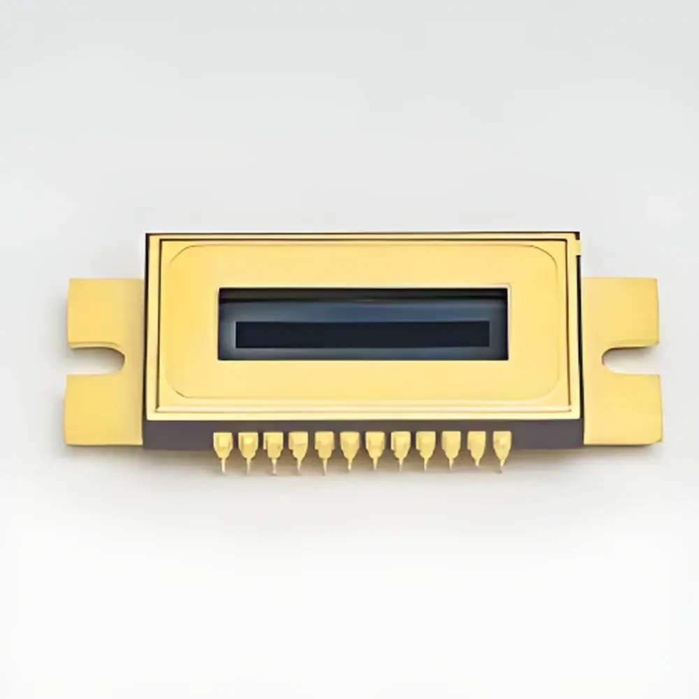
Hamamatsu Back-Illuminated CCD Area Image Sensor S10141-1107S-01
| Brand | Hamamatsu |
|---|---|
| Origin | Japan |
| Manufacturer Type | Original Equipment Manufacturer (OEM) |
| Origin Category | Imported |
| Model | S10141-1107S-01 |
| Price Range | USD 0–9,999 |
Overview
The Hamamatsu S10141-1107S-01 is a scientific-grade, back-illuminated charge-coupled device (CCD) area image sensor engineered for high-fidelity spectral detection in low-light analytical environments. Based on full-frame transfer architecture with on-chip binning capability, it operates via photonic integration of incident photons into electron charge packets within silicon photodiodes, followed by serial charge transfer and low-noise correlated double sampling (CDS) readout. Its back-illuminated design eliminates gate structure absorption, enabling quantum efficiency exceeding 90% at peak wavelengths—particularly critical for UV–NIR spectroscopic applications where photon budgets are constrained. The sensor’s 12 µm × 12 µm pixel pitch supports spatial resolution up to 2048 × 122 active pixels (24.576 mm × 1.464 mm photosensitive area), optimized for compact spectrometer integration, monochromator-based systems, and multi-channel optical detection platforms requiring stable, reproducible intensity linearity across 200–1100 nm.
Key Features
- Back-illuminated architecture with anti-reflection coated sapphire window for enhanced UV transmission and long-term environmental stability
- Ultra-low readout noise: 4 e⁻ rms (typical), achieved through optimized CDS circuitry and on-chip clock driver design
- Multi-pinned phase (MPP) operational mode enabling dark current suppression to 30 e⁻/pixel/s (typical, Ta = 25 °C), essential for extended integration times
- Single-stage thermoelectric (TE) cooling integrated into metal package, reducing thermal noise without requiring external chillers or liquid nitrogen
- Full-line binning support: configurable vertical binning to emulate high-sensitivity linear array behavior while retaining area-imaging flexibility
- Saturation charge capacity of 70 ke⁻ (typical), delivering wide dynamic range (>90 dB) suitable for quantitative absorbance and emission measurements
- PIN-compatible footprint with Hamamatsu S7030/S7031 series, facilitating drop-in replacement in legacy OEM spectroscopy modules
Sample Compatibility & Compliance
The S10141-1107S-01 is designed for integration into ISO/IEC 17025-accredited analytical instrumentation and complies with RoHS Directive 2011/65/EU and REACH Regulation (EC) No. 1907/2006. Its spectral response (200–1100 nm) supports compliance with ASTM E308-22 (computing colorimetric data), ISO 13406-2 (display measurement), and USP (UV–vis spectrophotometer verification). The TE-cooled metal package ensures mechanical robustness under vibration and thermal cycling conditions typical of benchtop and portable spectrometers. No internal battery or hazardous substances are used; the device is intended for fixed-installation use within Class I laser safety enclosures per IEC 60825-1.
Software & Data Management
The sensor interfaces via standard LVDS or CMOS parallel output protocols (configurable per OEM requirements), supporting synchronization with external trigger signals and programmable exposure timing down to sub-millisecond resolution. When integrated with Hamamatsu’s DCAM-SDK or third-party libraries (e.g., HALCON, LabVIEW Vision Acquisition Software), it enables automated gain calibration, non-uniformity correction (NUC), and frame averaging—features required for GLP/GMP traceability. Audit trails, timestamped metadata embedding, and raw 16-bit linear output ensure compatibility with FDA 21 CFR Part 11–compliant data acquisition systems when deployed in regulated pharmaceutical or clinical chemistry workflows.
Applications
- UV–vis–NIR spectrophotometers and microplate readers requiring high SNR in low-concentration absorbance assays
- Raman spectroscopy detection modules where stray-light rejection and UV quantum efficiency directly impact signal fidelity
- Fluorescence lifetime imaging (FLIM) and time-resolved luminescence systems leveraging MPP-mode dark current control
- OEM engine analyzers and combustion diagnostics using broadband emission spectroscopy
- Astronomical instrumentation calibration sources and laboratory reference spectrometers
- Environmental monitoring sensors for dissolved organic carbon (DOC) and nitrate detection in water quality analyzers
FAQ
What integration time ranges are supported in MPP mode?
Typical integration spans 1 ms to 60 s, limited only by dark current accumulation and host controller buffer capacity.
Is vacuum packaging available for ultra-high-vacuum spectrometer integration?
No—this variant uses hermetically sealed metal housing with sapphire window; custom vacuum-compatible variants (e.g., S10141-1107V) require direct OEM consultation.
Does the sensor support region-of-interest (ROI) readout?
No—full-frame or vertically binned readout only; ROI functionality requires external FPGA-based pixel masking.
What is the maximum frame rate with full 2048 × 122 resolution?
107 lines/s (typical) at full resolution; 203 lines/s achievable with partial binning and reduced bit depth.
Can this sensor be operated without TE cooling?
Yes—ambient operation is possible but increases dark current exponentially above 30 °C; TE cooling is recommended for quantitative applications requiring <0.1% photometric repeatability.
Related Products

")