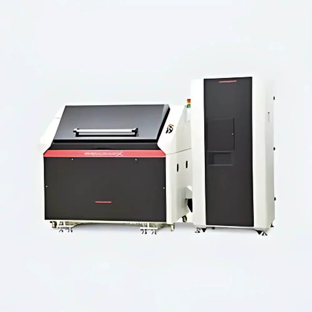
Hamamatsu iPHEMOS-MPX Inverted Photoluminescence and Thermal Emission Microscope C10506-07-06
| Brand | Hamamatsu |
|---|---|
| Origin | Japan |
| Manufacturer | Hamamatsu Photonics K.K. |
| Type | Imported Instrument |
| Model | C10506-07-06 |
| Pricing | Upon Request |
Overview
The Hamamatsu iPHEMOS-MPX is an inverted photoluminescence and thermal emission microscope engineered for high-precision failure analysis (FA) of advanced semiconductor devices. It operates on the principle of detecting ultra-weak photon emissions—such as electroluminescence (EL), photoluminescence (PL), and thermally activated photon emission (TAP)—originating from localized defects, leakage paths, or hot carriers within integrated circuits under electrical bias or thermal stress. Unlike conventional optical microscopes, the iPHEMOS-MPX integrates dual-sensor detection architecture with wavelength-tailored optics to simultaneously acquire spatially registered luminescent and thermal signatures across broad spectral bands (typically 400–1700 nm), enabling unambiguous correlation between physical layout and failure physics. Its inverted optical configuration accommodates large-area probe stations, wafer-level test fixtures, and nano-positioning stages—making it suitable for front-side and back-side FA workflows on nodes down to 3 nm.
Key Features
- Dual high-sensitivity camera system: Supports independent mounting of two EMCCD or InGaAs-based detectors optimized for visible/NIR (e.g., 400–1000 nm) and SWIR (e.g., 900–1700 nm) spectral ranges, allowing concurrent photonic and thermal emission mapping.
- Multi-source excitation compatibility: Accommodates up to four external laser or LED sources—including OBIRCH (Optical Beam Induced Resistance Change), DALS (Delay Analysis of Light Signals), EOP (Electro-Optical Probing), and laser marking modules—for stimulus-synchronized defect activation and localization.
- Modular lens turret: Integrates up to ten objective lenses with calibrated magnifications (5× to 100×) and transmission-optimized coatings matched to detector quantum efficiency curves; includes dedicated micro-lens assemblies for high-numerical-aperture near-field imaging.
- Precision motorized XYZ stage: Features 60 mm × 60 mm × 20 mm travel range with sub-micron repeatability (±0.1 µm), compatible with standard probe station interfaces and optional NanoLens add-ons for diffraction-limited resolution enhancement.
- Real-time overlay engine: Fuses low-light emission images with high-resolution mask-layer reference images using sub-pixel registration algorithms, supporting automated defect centroid extraction and coordinate-based navigation in GDSII-aligned environments.
Sample Compatibility & Compliance
The iPHEMOS-MPX is designed for direct integration into semiconductor failure analysis laboratories operating under ISO/IEC 17025-accredited quality systems. It supports bare die, packaged ICs, wafers (up to 300 mm), and flip-chip assemblies mounted on commercial probe stations (e.g., Cascade Microtech, FormFactor). All optical and mechanical components comply with JIS B 7153 (optical instrument calibration) and IEC 61000-4-2 (ESD immunity). The system meets CE marking requirements for electromagnetic compatibility (EMC Directive 2014/30/EU) and low-voltage safety (LVD Directive 2014/35/EU). Optional TD Imaging module adheres to JEDEC JESD22-A121A (laser-induced fault isolation) and supports traceable calibration per NIST-traceable standards for quantitative photon flux measurement.
Software & Data Management
Control and analysis are managed via Hamamatsu’s FA-Studio Suite v5.x, a Windows-based application compliant with FDA 21 CFR Part 11 for electronic records and signatures. Core capabilities include time-resolved emission profiling (down to 1 ns gate resolution), spectral deconvolution of multi-wavelength datasets, and automated defect clustering using k-means segmentation. Audit trails record all user actions, parameter changes, and image processing steps with timestamped metadata. Data export supports TIFF (16-bit linear), HDF5 (for multi-dimensional time-spectral stacks), and CSV formats compatible with industry-standard FA workflow tools such as Synopsys TetraMAX and Keysight PathWave ADS. Integration with SEMI E142-compliant MES interfaces enables direct linkage to fab-level yield management systems.
Applications
- Identification of gate oxide shorts, junction leakage, and latch-up sites in FinFET and GAA transistor architectures.
- Localization of electromigration voids and resistive opens in Cu/low-k interconnect stacks.
- Back-side failure analysis of 2.5D/3D ICs using laser-assisted device thinning and through-silicon via (TSV) inspection.
- Dynamic fault imaging during functional testing (e.g., scan chain failure, timing violation-induced hot spots).
- Correlative analysis with SEM/FIB-SEM cross-sectioning by exporting precise XY coordinates with ±0.5 µm uncertainty.
FAQ
What types of semiconductor defects can iPHEMOS-MPX detect?
It detects optically active failure mechanisms including but not limited to gate-induced drain leakage (GIDL), impact ionization hot carriers, trap-assisted tunneling, and thermal runaway in power devices.
Is vacuum operation required?
No vacuum chamber is integrated; however, the system requires ambient pressure ≥80 kPa for stable cooling of InGaAs sensors and consistent optical path refractive index—standard lab environments meet this requirement.
Can the system be upgraded with additional light sources or detectors post-purchase?
Yes—modular design allows field-installation of new laser modules, filter wheels, and detector units via certified Hamamatsu service engineers, with firmware updates validated against ISO 13485 change control protocols.
Does TD Imaging require special sample preparation?
No. TD Imaging performs time-domain gating directly on live emission signals without metal layer removal or focused ion beam (FIB) milling—enabling non-destructive, in-situ analysis of fully packaged devices.
What is the typical spatial resolution achievable?
Lateral resolution is diffraction-limited by the selected objective lens and wavelength; at 900 nm with a 100×/0.9 NA objective, theoretical resolution is ~500 nm (FWHM), empirically verified using NIST SRM 2053 line-width standards.
Related Products


