Hamamatsu μAMOS Infrared Confocal Laser Failure Analysis System
| Brand | Hamamatsu |
|---|---|
| Origin | Japan |
| Manufacturer Type | Original Equipment Manufacturer (OEM) |
| Import Status | Imported |
| Model | μAMOS |
| Pricing | Upon Request |
| Laser Wavelength | 1.3 µm (standard), optional 1.1 µm pulsed or high-power 1.3 µm (>400 mW) |
| Spatial Resolution (Backside Imaging) | ≤0.26 µm (with 100× HR NIR objective) |
| Detection Method | Lock-in Amplified OBIRCH (Optical Beam Induced Resistance Change) |
| Voltage/Current Biasing | 4-Quadrant ±10 mV–±10 V / ±100 mA |
| Sample Compatibility | 200 mm / 300 mm wafers (front/backside), diced dies, packaged ICs with polished backside, EPI-substrates |
| Vacuum Requirement | ≥80 kPa |
| Compressed Air | 0.5–0.7 MPa |
| Power Supply | AC 220 V, 50/60 Hz, ~3000 W |
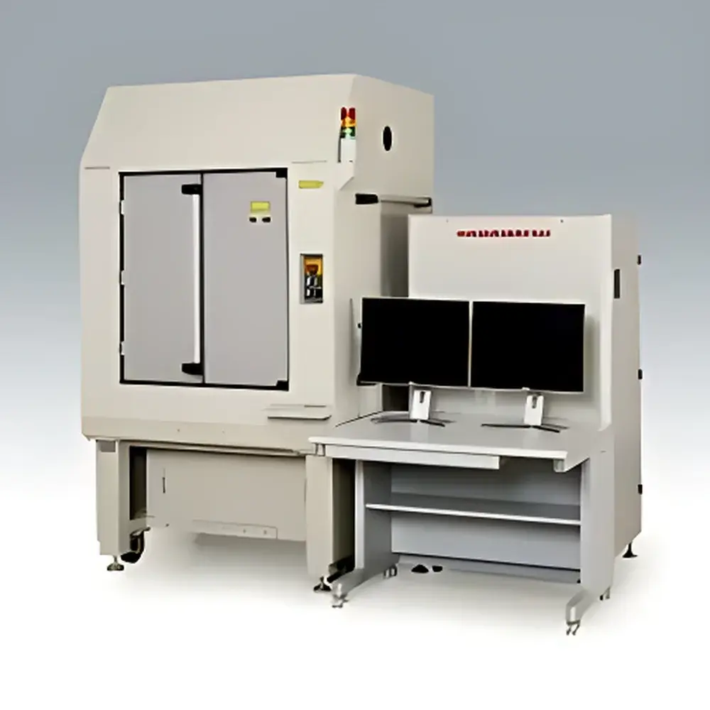
| Main Unit Dimensions | 1360 × 1410 × 2120 mm (W×D×H), ~900 kg |
| Control Console | 880 × 700 × 1542 mm, ~255 kg |
Overview
The Hamamatsu μAMOS Infrared Confocal Laser Failure Analysis System is a purpose-built, high-precision tool engineered for non-destructive, backside localization of electrical defects in advanced semiconductor devices. It operates on the principle of Optical Beam Induced Resistance Change (OBIRCH) using near-infrared (NIR) laser excitation at 1.3 µm — a wavelength specifically selected to achieve deep silicon penetration while avoiding optical beam induced current (OBIC) artifacts common with shorter-wavelength lasers. This enables unambiguous detection of resistive anomalies such as leakage paths, voids, electromigration damage, and high-resistance contacts in fully processed CMOS, FinFET, and 3D-stacked ICs. The system integrates confocal scanning optics, lock-in amplification, and synchronized four-quadrant voltage/current biasing to isolate weak OBIRCH signals from thermal and electronic noise—critical for IDDQ (quiescent supply current) failure analysis where leakage currents fall below 1 nA. Its mechanical architecture supports both wafer-level (200 mm / 300 mm) and packaged device analysis, including flip-chip and TSV-based packages with mirror-polished silicon backsides.
Key Features
- Confocal infrared laser scanning with selectable 1.3 µm continuous-wave diode laser (100 mW standard; >400 mW optional) or 1.1 µm pulsed laser (800 mW peak power) for enhanced thermal contrast in high-doping substrates.
- Lock-in amplifier integration synchronized with laser modulation frequency, delivering >60 dB signal-to-noise ratio improvement over DC detection—essential for sub-picoampere leakage localization.
- High-NA NIR-optimized objective turret supporting up to five objectives, including M-PLAN-NIR-100×HR (NA 0.70, WD 10 mm) and G-PLAN-APO-NIR-100×HR (NA 0.70, WD 6 mm), enabling spatial resolution down to 0.13 µm (lateral) at 1.3 µm wavelength.
- Full four-quadrant biasing capability: programmable voltage sweep (±10 mV to ±25 V) and current sourcing/sinking (±100 µA to ±100 mA), with real-time monitoring of V/I response during OBIRCH acquisition.
- Dedicated microcurrent preamplifier (23 pA input noise floor) and low-noise voltage amplifier (11 µV RMS) for quantitative defect characterization under minimal stress conditions.
- Motorized XYZ stage with ±20 mm X/Y travel and 75 mm Z-focus range, calibrated for thermal drift compensation and compatible with probe station integration (e.g., Cascade Summit, Micromanipulator).
Sample Compatibility & Compliance
The μAMOS accommodates a broad spectrum of semiconductor specimens without front-side deprocessing: diced dies (post-dicing), full 200 mm and 300 mm wafers (front- or backside accessible), and packaged ICs requiring only backside polishing to <1 µm surface roughness. It is validated for use with epitaxial (EPI) substrates, SOI wafers, and high-resistivity silicon—materials where conventional visible-light OBIRCH fails due to absorption or scattering. The system conforms to industry-standard environmental and safety requirements, including IEC 61000-6-3 (EMC emission), IEC 61000-6-2 (immunity), and JIS C 61010-1 for laboratory electrical safety. While not certified to ISO/IEC 17025, its measurement traceability aligns with internal calibration protocols referenced to NIST-traceable photodiode responsivity standards and Keithley 2450 SourceMeter® voltage/current references. Data acquisition workflows support GLP-compliant audit trails when integrated with Hamamatsu’s optional LabVIEW-based control suite.
Software & Data Management
Control and analysis are executed via Hamamatsu’s proprietary μAMOS Acquisition Suite, a Windows-based application built on modular LabVIEW architecture. It provides synchronized laser modulation, stage positioning, lock-in parameter tuning (time constant, phase, filter slope), and real-time OBIRCH image formation (512×512 in ≤12 s; 1024×1024 in ≤48 s). All raw and processed data—including voltage maps, current maps, resistance-change overlays, and time-domain transient traces—are stored in HDF5 format with embedded metadata (laser power, objective ID, bias settings, timestamp, operator ID). Export options include TIFF, CSV, and MATLAB .mat for cross-platform correlation with SPICE simulations or CAD layout tools (e.g., Calibre RVE). Optional FDA 21 CFR Part 11 compliance package adds electronic signature enforcement, role-based access control, and immutable audit logs for regulated environments.
Applications
- IDDQ failure root cause analysis in logic and memory ICs, isolating gate oxide pinholes, junction leakage, and latch-up initiation sites.
- Metallization defect detection: voids in Cu interconnects, poor via/trench fill, and TiN barrier discontinuities in sub-7 nm nodes.
- Backside fault isolation in 2.5D/3D ICs, including TSV resistance anomalies and microbump contact failures.
- Process development feedback for CMP uniformity, anneal optimization, and silicide formation—via correlation of OBIRCH contrast intensity with sheet resistance maps.
- Reliability stress testing: real-time OBIRCH monitoring during HTOL (high-temperature operating life) or ESD qualification to capture progressive degradation mechanisms.
FAQ
Can μAMOS analyze fully packaged flip-chip devices?
Yes—provided the silicon backside is polished to optical grade (Ra < 1 nm) and free of metal layers or dielectric stacks thicker than 5 µm. Standard configurations support up to 1 mm substrate thickness.
What is the minimum detectable leakage current under OBIRCH mode?
With lock-in amplification and the optional microcurrent amplifier, the system resolves resistance changes corresponding to ~100 fA static leakage under optimized bias and averaging (128-frame accumulation, 1 s dwell/pixel).
Is vacuum required for all measurements?
Vacuum (≥80 kPa) is mandatory only during high-resolution imaging with long-working-distance objectives to minimize thermal lensing and air convection artifacts; atmospheric operation is supported for coarse survey scans.
Does μAMOS support automated defect review after hotspot detection?
Yes—the software includes scriptable ROI navigation and can interface with third-party SEM/FIB systems via SECS/GEM protocol for correlative structural analysis.
Are calibration certificates provided with the system?
Hamamatsu supplies factory calibration reports for laser power output, stage positioning accuracy (±0.1 µm), and amplifier gain linearity. On-site metrology verification services are available under separate contract.


