Hefei Kejing SrTiO3 Single-Crystal Substrates
| Brand | Hefei Kejing |
|---|---|
| Origin | Anhui, China |
| Manufacturer Type | Authorized Distributor |
| Product Origin | Domestic (China) |
| Model | SrTiO3 |
| Crystal Structure | Cubic |
| Lattice Constant | a = 3.905 Å |
| Growth Method | Flame Fusion (Verneuil) |
| Melting Point | 2080 °C |
| Density | 5.175 g/cm³ |
| Mohs Hardness | 6 |
| Thermal Expansion Coefficient | 9.4 × 10⁻⁶ /°C |
| Dielectric Constant | ~300 |
| Loss Tangent | ~5 × 10⁻⁴ @ 300 K, ~3 × 10⁻⁴ @ 77 K |
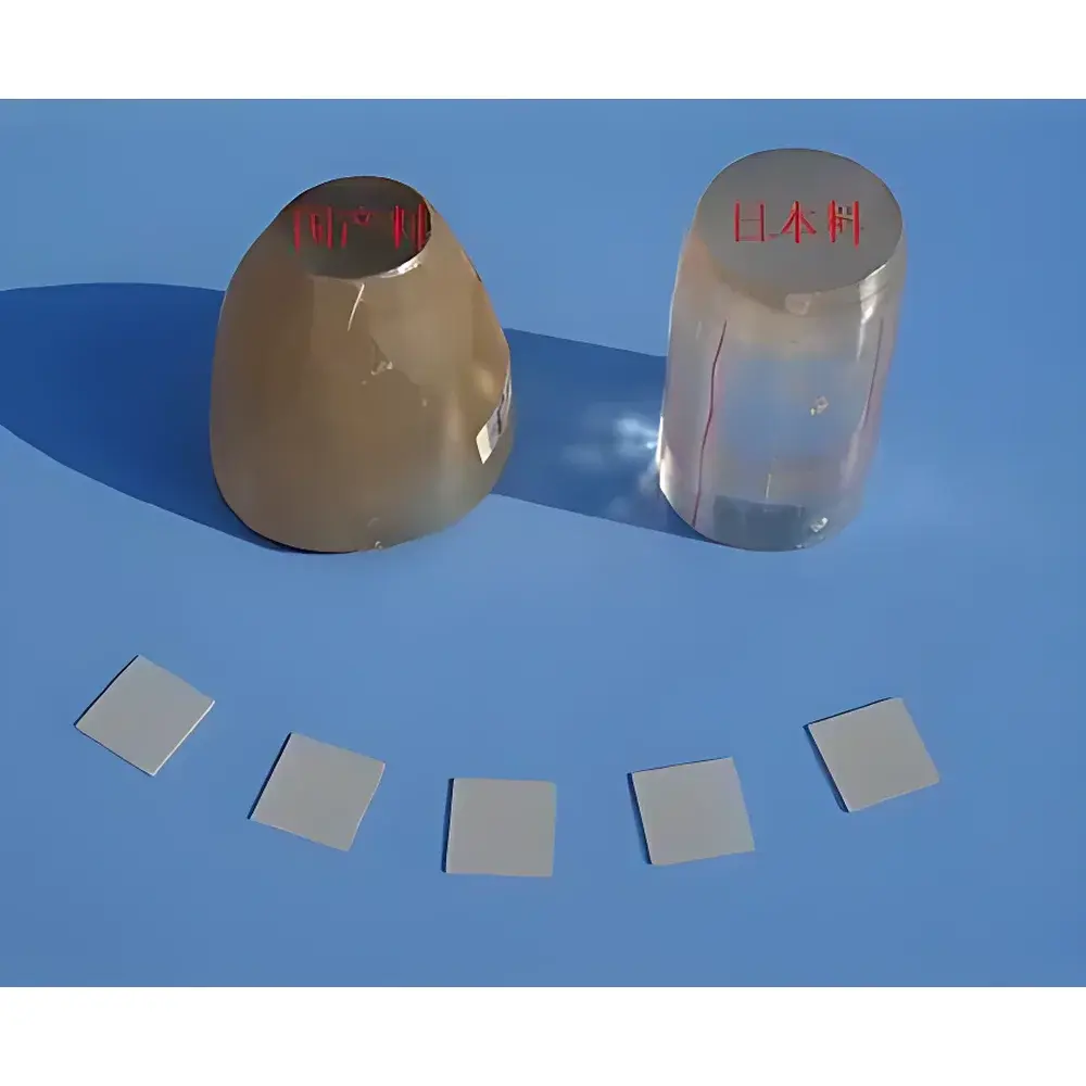
| Surface Finish | Single- or Double-Polished |
| Surface Roughness (Ra) | < 0.5 nm |
| Orientation Tolerance | ±0.5° |
| Standard Dimensions | Ø30 × 0.5 mm, 10 × 10 × 0.5 mm, 10 × 5 × 0.5 mm, 5 × 5 × 0.5 mm |
| Available Orientations | <100>, <110>, <111> |
| Chemical Stability | Insoluble in water |
| Packaging | Plasma-cleaned in ISO Class 6 (1000-grade) cleanroom, sealed in ISO Class 5 (100-grade) laminar flow bags |
Overview
Hefei Kejing SrTiO₃ single-crystal substrates are high-purity, orientation-controlled perovskite oxide wafers engineered for epitaxial thin-film growth and advanced electrochemical and optical applications. As a cubic perovskite with lattice parameter a = 3.905 Å, SrTiO₃ exhibits exceptional structural compatibility with a wide range of functional oxides—including high-temperature superconductors (e.g., YBCO), complex transition-metal oxides (e.g., LSMO, LCO), and ferroelectric or multiferroic films (e.g., BiFeO₃, PZT). Its low dielectric loss (<5 × 10⁻⁴ at 300 K), high dielectric constant (~300), and thermal expansion coefficient (9.4 × 10⁻⁶ /°C) enable stable interfacial strain control during pulsed laser deposition (PLD), sputtering, and molecular beam epitaxy (MBE). The substrates are grown via the flame fusion (Verneuil) method—ensuring stoichiometric homogeneity, minimal point defects, and absence of twins—followed by precision mechanical lapping, chemical-mechanical polishing (CMP), and atomic-level surface finishing (Ra < 0.5 nm). These attributes make them indispensable as seed layers, dielectric gate insulators, QCM electrodes, and optical windows in cryogenic and UHV-compatible instrumentation.
Key Features
- Cubic perovskite structure with precise lattice matching to >20 common oxide thin-film systems
- Orientation accuracy maintained within ±0.5° for , , and crystallographic planes
- Double-polished surfaces with RMS roughness <0.5 nm (Ra), verified by AFM and optical interferometry
- Plasma-cleaned and packaged in ISO Class 5 (100-grade) cleanroom bags following ISO 14644-1 protocols
- Thermally stable up to 2080 °C; compatible with in-situ annealing and high-temperature deposition processes
- Available in standardized geometries (Ø30 × 0.5 mm, 10 × 10 × 0.5 mm, etc.) and custom dimensions upon request
Sample Compatibility & Compliance
These substrates are routinely used in certified thin-film fabrication workflows compliant with ASTM F394 (Standard Guide for Characterization of Epitaxial Thin Films), ISO/IEC 17025-accredited metrology labs, and GLP/GMP-aligned R&D environments. Their chemical inertness—insolubility in water and resistance to mild acidic/basic etchants—ensures long-term stability during electrochemical cell assembly and QCM sensor integration. All batches undergo full crystallographic verification via X-ray diffraction (XRD) rocking curve analysis (FWHM < 0.02° for orientation), ensuring reproducibility across production runs. Trace metal impurities (Fe, Ni, Cr) are controlled below 1 ppm per ICP-MS assay, meeting stringent requirements for quantum materials synthesis.
Software & Data Management
While SrTiO₃ substrates themselves are passive components, they interface directly with instrument control platforms used in thin-film deposition systems (e.g., Oxford Instruments Ionfab, Kurt J. Lesker CMS series) and electrochemical workstations (e.g., BioLogic SP-300, Metrohm Autolab PGSTAT302N). Batch-specific certification data—including XRD θ–2θ scans, AFM topographs, and surface contamination reports (via TOF-SIMS)—are provided in machine-readable CSV and PDF formats. Traceability is ensured through unique lot numbering aligned with ISO 9001:2015 documentation standards, supporting audit readiness for FDA 21 CFR Part 11-compliant electronic records in regulated development settings.
Applications
- Epitaxial template for high-Tc superconducting films (YBa₂Cu₃O7−δ, La₂₋xSrxCuO₄)
- Dielectric layer in oxide-based capacitors and ferroelectric tunnel junctions
- Substrate for resistive switching memristors and 2D oxide heterostructures
- Electrode platform for quartz crystal microbalance (QCM-D) biosensing and interfacial electrochemistry
- Optical window material for mid-IR transmission spectroscopy (transparency range: 0.3–6 µm)
- Target material precursor for reactive sputtering of STO-based thin films
FAQ
What surface finish options are available?
Standard offerings include single-side polished (SSP) and double-side polished (DSP) variants, both achieving Ra < 0.5 nm. Custom finishes—including ion-beam smoothing or conductive Nb-doped STO variants—are available under NDA.
Can substrates be supplied with pre-deposited seed layers?
Yes—Hefei Kejing collaborates with certified thin-film foundries to provide STO substrates with pre-grown buffer layers (e.g., TiN, LaNiO₃, or SrRuO₃) under controlled UHV conditions.
Are certificates of analysis (CoA) provided with each shipment?
Each lot includes a CoA detailing XRD orientation confirmation, surface roughness (AFM), impurity profile (ICP-MS), and packaging compliance (ISO Class 5 bag integrity test report).
Do you support wafer-level metrology integration?
Yes—substrates are compatible with automated handling in cluster tools and can be supplied with SEMI-standard notches or flats for robotic alignment in semiconductor-grade processing lines.