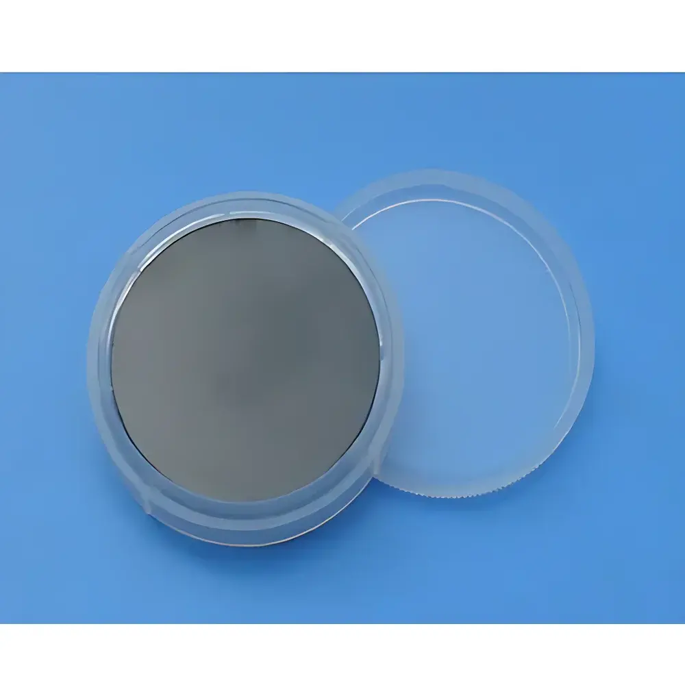
MgO-Buffered YBCO High-Temperature Superconducting Thin Film
| Brand | Hefei Kejing |
|---|---|
| Origin | Anhui, China |
| Manufacturer Type | Authorized Distributor |
| Origin Category | Domestic |
| Model | MgO+YBCO Superconducting Thin Film |
| Pricing | Available Upon Request |
| Microwave Surface Resistance (Rs) | <0.5 mΩ @ 77 K, 10 GHz |
| Critical Current Density (Jc) | >2 MA/cm² @ 77 K, 0 T |
| Thickness | 100–1000 nm (standard: 300 nm), double-sided deposition |
| Thickness Uniformity | ±4% across wafer |
| Substrate Diameter | 2" or 3" |
| Surface Finish | Single-side or double-side polished |
| Packaging | Vacuum-sealed in Class 100 cleanroom bags within Class 1000 cleanroom environment, or individual cassette packaging |
Overview
The MgO-buffered YBCO (Yttrium Barium Copper Oxide) high-temperature superconducting thin film is a precision-engineered functional material designed for cryogenic microwave and quantum electronic applications. Fabricated via pulsed laser deposition (PLD) or sputtering on single-crystal MgO substrates, the film leverages epitaxial growth to achieve high crystallinity and low defect density—critical for minimizing microwave surface resistance and maximizing critical current density. Operating at liquid nitrogen temperature (77 K), this YBCO film eliminates the need for costly liquid helium cooling while delivering performance metrics comparable to low-temperature superconductors in specific frequency bands. Its intrinsic properties—low Rs, high Jc, and excellent thickness uniformity—make it suitable for integration into planar superconducting circuits where phase coherence, signal integrity, and thermal stability are paramount.
Key Features
- Low microwave surface resistance: <0.5 mΩ at 77 K and 10 GHz—enabling high-Q resonant structures and low-loss passive components
- Critical current density exceeding 2 MA/cm² under zero magnetic field at 77 K—supporting high-power handling in Josephson junctions and DC SQUIDs
- Controlled thickness range of 100–1000 nm with standard 300 nm deposition; double-sided film configuration available for symmetric device architectures
- Thickness uniformity maintained within ±4% across full 2-inch or 3-inch diameter wafers—ensuring batch-to-batch reproducibility in photolithographic processing
- Substrate options include single-side or double-side polished MgO wafers with atomically flat surfaces (RMS roughness <0.2 nm), optimized for subsequent lift-off or etch-based patterning
- Class 100 cleanroom vacuum packaging in 100-grade sealed bags—preserving surface stoichiometry and preventing moisture-induced degradation during storage and transport
Sample Compatibility & Compliance
This YBCO thin film is compatible with standard microfabrication workflows including photolithography, ion milling, reactive ion etching (RIE), and lift-off metallization. The MgO substrate exhibits excellent lattice matching with YBCO (mismatch <1%), resulting in high-quality c-axis oriented films with minimal twin-domain formation. All wafers undergo post-deposition annealing in controlled oxygen partial pressure environments to ensure optimal oxygen stoichiometry—a requirement for achieving reproducible superconducting transition temperatures (Tc > 89 K). While not certified to ISO/IEC 17025 or ASTM F2628 (standard for HTS film characterization), the product conforms to widely accepted industry benchmarks for microwave Rs and Jc measurement protocols defined in IEEE Std 1652™ and the NIST HTS Characterization Guidelines. Traceable calibration data—including four-point probe resistivity mapping and SQUID magnetometry reports—can be provided upon request for GLP-compliant research environments.
Software & Data Management
As a passive thin-film material—not an instrument—the MgO+YBCO film does not include embedded firmware or proprietary software. However, its metrological characteristics are fully compatible with industry-standard characterization platforms: Keysight PNA-X network analyzers (for Rs extraction via coplanar waveguide measurements), Quantum Design MPMS3 or PPMS systems (for magnetotransport and M–H loop analysis), and Bruker D8 Discover XRD (for structural phase identification and out-of-plane texture assessment). Raw data generated from such instruments may be managed using open-format tools compliant with FAIR principles (Findable, Accessible, Interoperable, Reusable), including HDF5, CSV, and TDMS export capabilities. For laboratories operating under FDA 21 CFR Part 11 or EU Annex 11 requirements, audit trails for film lot traceability, environmental exposure logs, and packaging integrity records can be maintained through LIMS-integrated documentation workflows.
Applications
- High-performance microwave filters and bandpass resonators for base-station front-end modules and satellite communication receivers
- Ultra-low-noise superconducting quantum interference device (SQUID) magnetometers and gradiometers for biomagnetic imaging (e.g., MEG)
- Josephson junction arrays used in programmable voltage standards and quantum current sources
- Infrared bolometric detectors leveraging the sharp superconducting-to-normal transition for high responsivity at cryogenic operating points
- Delay lines and phase shifters in phased-array radar subsystems requiring sub-picosecond timing jitter and minimal dispersion
- Test vehicles for fundamental studies of vortex dynamics, flux pinning mechanisms, and proximity effects in hybrid superconductor–topological insulator heterostructures
FAQ
What is the typical transition temperature (Tc) of this YBCO film?
The onset Tc typically exceeds 90 K, with midpoint Tc values centered at 89.2 ± 0.3 K, as verified by magneto-resistive transition scans under zero-field conditions.
Can these films be patterned using standard optical lithography?
Yes—they are fully compatible with i-line (365 nm) and deep-UV (248 nm) photolithography, followed by Ar-ion milling or wet etching in dilute HCl/HNO3 solutions.
Is substrate removal or transfer to alternative platforms (e.g., Si, sapphire) supported?
Laser lift-off or chemical etch-release processes have been demonstrated in peer-reviewed literature; however, Kejing-supplied wafers are delivered in as-deposited configuration on MgO substrates only.
Do you provide certificate of conformance or material test reports?
Lot-specific test reports—including Rs maps, Jc histograms, XRD θ–2θ scans, and AFM topography—are available upon formal request and subject to NDA execution.
What is the shelf life under recommended storage conditions?
When stored desiccated at room temperature in original vacuum packaging, functional integrity is guaranteed for ≥12 months; prolonged exposure to ambient humidity degrades surface oxygen content and increases Rs.