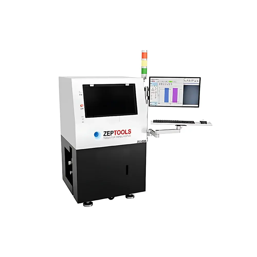
ZEPTOOLS JS100B Semi-Automatic Profilometer
| Brand | ZEPTOOLS |
|---|---|
| Model | JS100B |
| Origin | Anhui, China |
| Probe Tip Radius | ≥2 µm (60° included angle, standard) |
| Probe Normal Force Range | 0.5–50 mg |
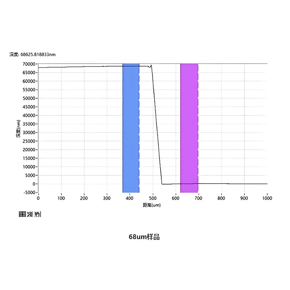
| Scan Length | 55 mm |
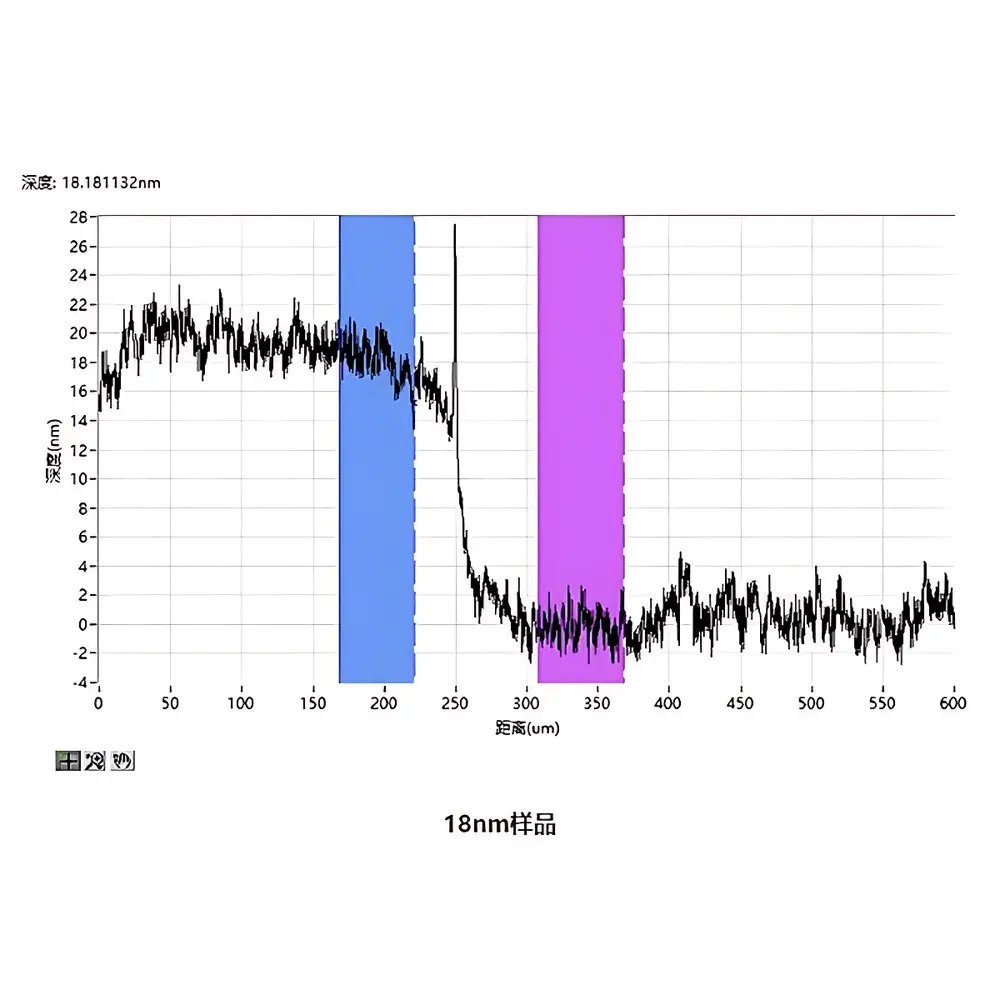
| Step Height Repeatability | ≤0.5 nm (1σ, 30 scans on 1 µm step standard) |
| Vertical Resolution | 0.05 nm (full scale) |
| Maximum Sample Dimensions | ≤150 mm × ≤200 mm × ≤300 mm |
| Measurement Accuracy | ±3 µm |
| Sampling Rate | 200 Hz |
| Scan Speed | 5–100 µm/s |
| XY Stage Travel | 150 mm × 200 mm (motorized) |
| XY Repeatability | ±3 µm |
| Z-Stage Travel | 10 mm |
| Rotary Stage | ±360°, 0.01° resolution |
Overview
The ZEPTOOLS JS100B Semi-Automatic Profilometer is a contact-mode surface topography measurement system engineered for precision step height, film thickness, surface roughness, waviness, and stress characterization at the micro- and nanoscale. Based on the established principle of stylus profilometry—where a diamond-tipped probe physically traverses the sample surface to transduce vertical displacement into high-fidelity analog signals—the JS100B integrates a closed-loop force regulation mechanism, sub-nanometer vertical resolution, and motorized multi-axis positioning to deliver metrologically traceable results in R&D and production environments. Its mechanical architecture adheres to ISO 25178-601 (areal surface texture) and ASTM E1043 (stylus profiling) foundational practices, supporting calibration traceability to NIST-traceable step standards. Designed specifically for laboratories requiring robust, repeatable contact-based metrology without the complexity or cost of fully automated platforms, the JS100B bridges the gap between manual benchtop profilers and industrial-grade coordinate measuring machines.
Key Features
- Sub-nanometer vertical resolution (0.05 nm full-scale) enabled by low-noise capacitive displacement sensing and real-time thermal drift compensation.
- Programmable probe normal force control (0.5–50 mg range) with active feedback stabilization—critical for preserving integrity of soft polymers, photoresists, and low-modulus thin films.
- Motorized XYZR stage system: 150 mm × 200 mm XY travel with ±3 µm repeatability; 10 mm Z travel; 360° rotary stage with 0.01° angular resolution for oblique feature alignment.
- Integrated coaxial optical imaging system (5 MP CMOS) with adjustable magnification and real-time overlay of probe tip position relative to region-of-interest—eliminating blind scanning and reducing setup time by up to 40%.
- Modular hardware design supporting field-upgradable components including sub-micron radius probes (≤1 µm tip radius, 60° included angle, optional), extended Z-range sensors, and vacuum-compatible stages.
- Built-in environmental monitoring (temperature, humidity) logged alongside measurement data to support GLP-compliant reporting and long-term stability analysis.
Sample Compatibility & Compliance
The JS100B accommodates wafers and substrates up to 150 mm × 200 mm × 300 mm (L×W×H), with maximum sample thickness of 10 mm (customizable). It supports rigid and semi-rigid materials including silicon, sapphire, fused silica, metal alloys, ceramics, and polymer films—provided surface hardness exceeds 100 HV to prevent probe-induced deformation. All measurements comply with ISO 4287 (profile roughness parameters), ISO 4288 (assessment of surface texture), and ASTM B487 (metallic coating thickness via stylus). For regulated industries, the system supports audit-ready data export (CSV, X3P, ISO 5436-2) and optional 21 CFR Part 11–compliant software modules with electronic signatures, role-based access control, and immutable audit trails.
Software & Data Management
ZEPTOOLS ProfilSoft v4.2 provides an intuitive, scriptable interface for single-point, line-scan, grid-based 3D mapping, and automated multi-site measurement routines. Core analytical functions include ISO 25178–compliant Sa/Sq/Sz calculation, step height extraction with edge-detection algorithms (Gaussian derivative, threshold-based), film thickness derivation from dual-step profiles, and curvature-based stress modeling per Stoney’s equation. Raw data is stored in vendor-neutral HDF5 format with embedded metadata (timestamp, operator ID, environmental conditions, calibration history). Batch processing, statistical process control (SPC) charting, and API integration (Python, LabVIEW) enable seamless inclusion into enterprise MES or LIMS workflows.
Applications
- Thin-film metrology: Quantifying deposition/etch depth in SiO₂, SiNₓ, ITO, and Al₂O₃ layers across semiconductor, MEMS, and display fabrication lines.
- Surface quality validation: Measuring Ra, Rq, Rz, and bearing ratio curves on machined automotive components, orthopedic implants, and optical lens molds.
- Process development: Monitoring wafer warpage, film stress evolution, and lithographic resist profile fidelity during process optimization.
- Failure analysis: Characterizing delamination edges, crack propagation morphology, and interfacial step discontinuities in packaging and bonding structures.
- Academic research: Supporting NSF- and ERC-funded projects in nanomanufacturing, 2D material transfer, and bio-interface engineering where traceable, non-optical topography is required.
FAQ
What standards does the JS100B support for calibration and reporting?
The system is compatible with ISO 5436-1 step height standards and NIST-traceable calibration artifacts. Certificate of Conformance includes uncertainty budgets per GUM (JCGM 100:2008) and supports ISO/IEC 17025 documentation requirements.
Can the JS100B measure transparent or highly reflective surfaces?
Yes—unlike optical interferometers, contact profilometry is insensitive to optical properties. However, proper probe selection and force tuning are essential to avoid scratching anti-reflective coatings or brittle oxides.
Is remote operation or network deployment supported?
Standard Ethernet (TCP/IP) and USB 3.0 interfaces enable remote desktop control and integration into lab-wide instrument networks. Optional OPC UA server module allows real-time data streaming to SCADA or cloud analytics platforms.
How is measurement traceability maintained over time?
Each system ships with a certified reference standard (1 µm Si step), and ProfilSoft includes automated daily verification routines. Calibration intervals are configurable per ISO/IEC 17025 internal procedures, with logs archived alongside raw datasets.
Does the JS100B meet FDA or medical device manufacturing requirements?
With optional 21 CFR Part 11 software licensing, the platform satisfies design control (21 CFR 820.30) and production record retention (21 CFR 820.180) mandates for Class II/III device manufacturers conducting surface finish validation.