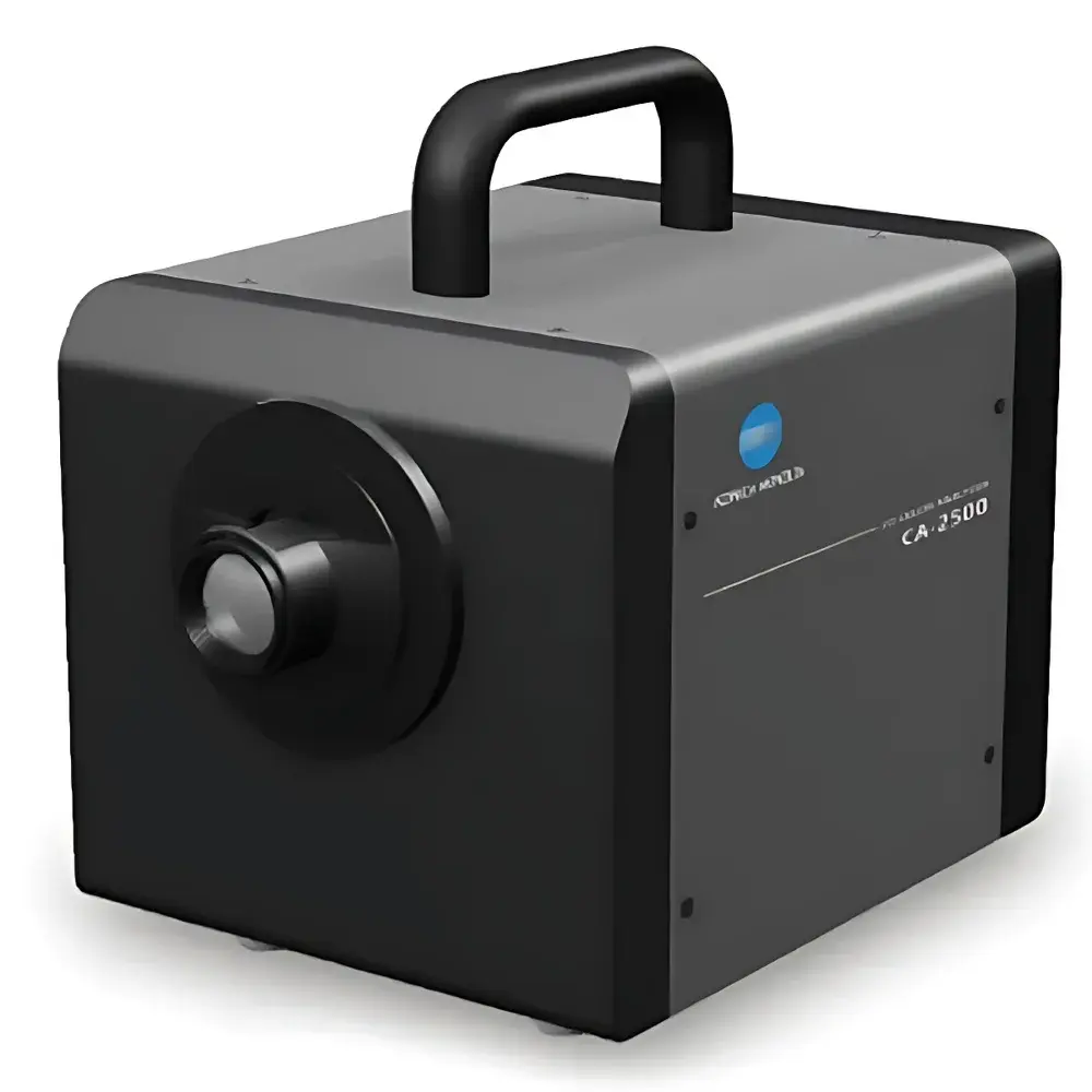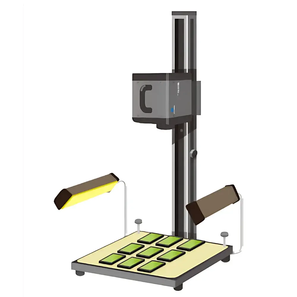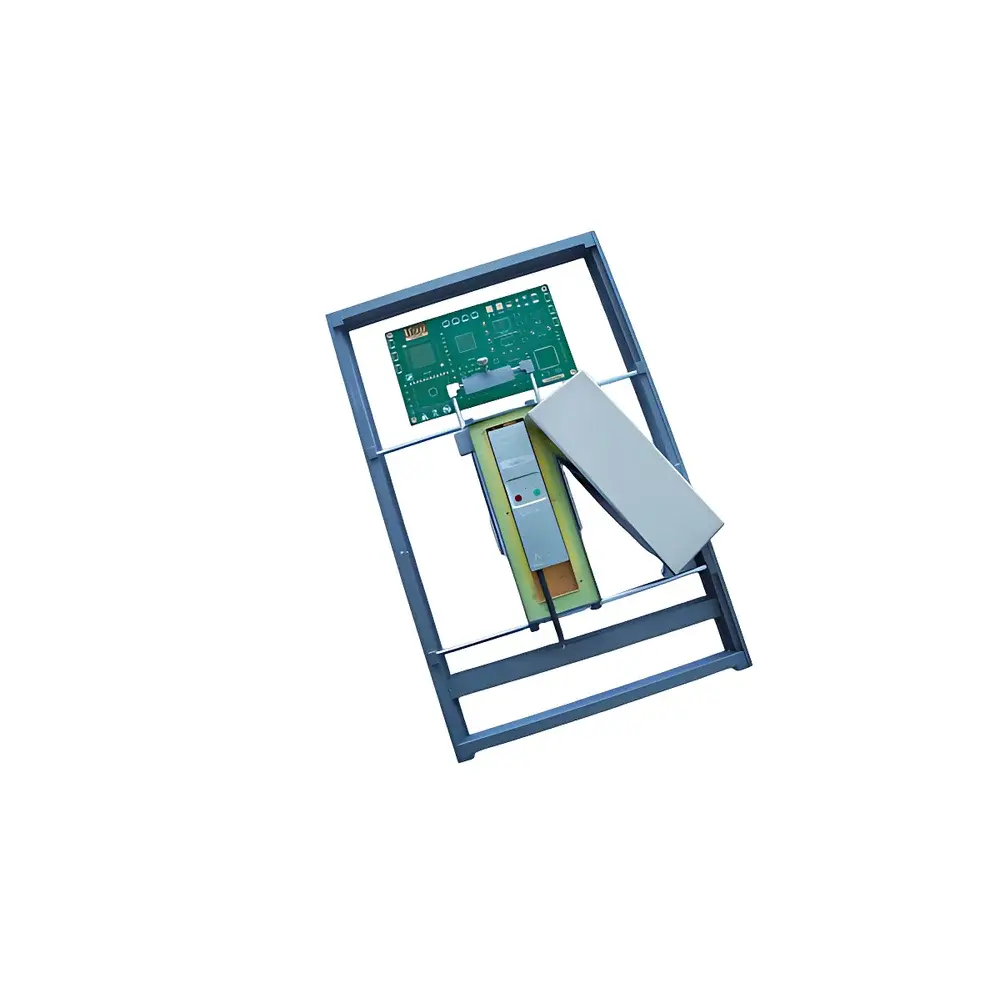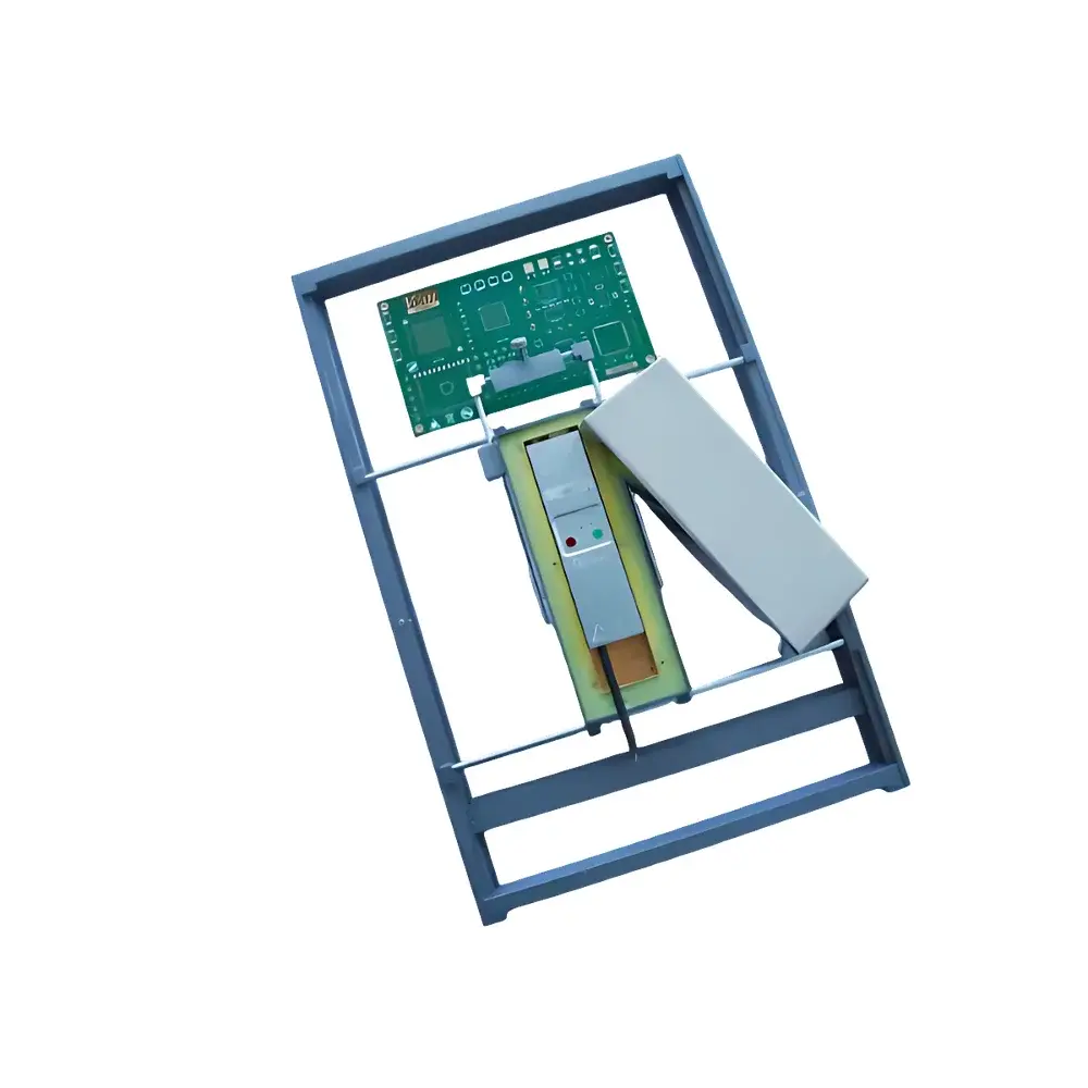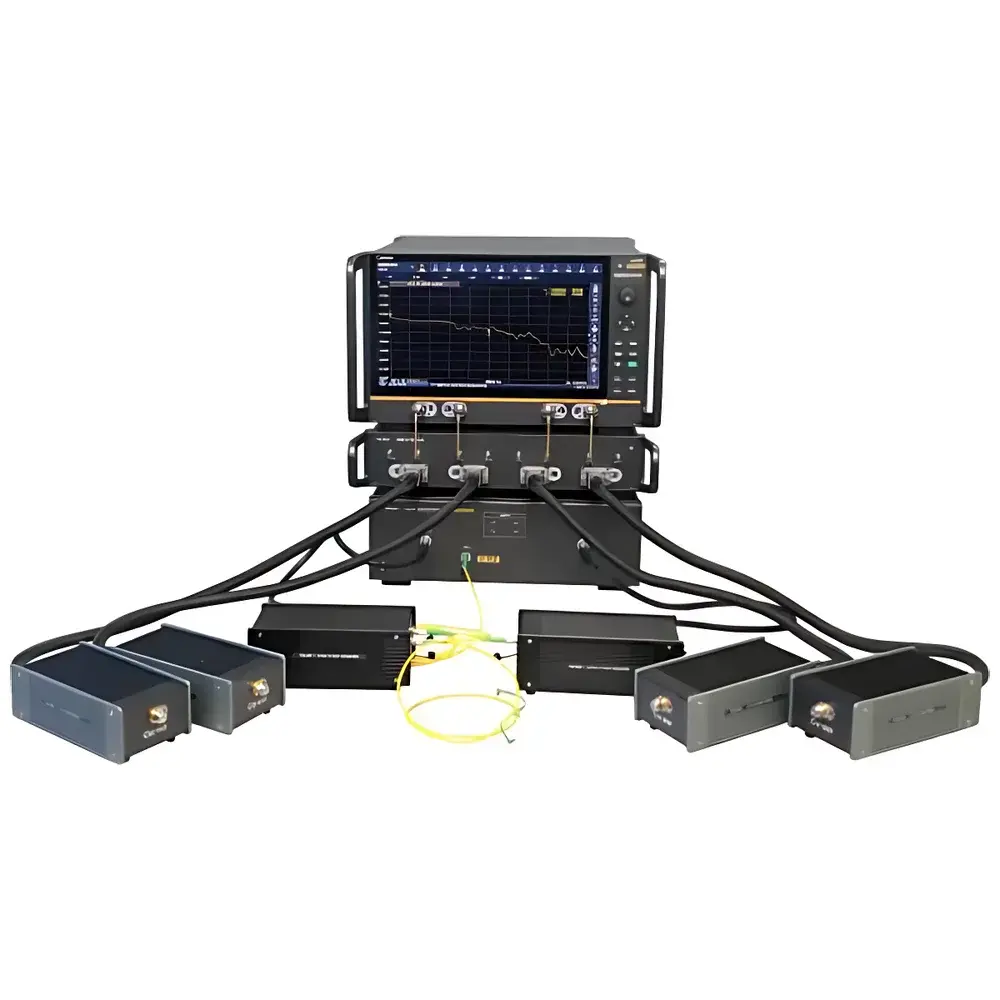
Auniontech 6433P Optical Wave Component Analyzer (10 MHz to 110 GHz Modulation Frequency Range)
| Brand | Auniontech |
|---|---|
| Origin | Shanghai, China |
| Model | 6433P |
| Frequency Range | 10 MHz – 110 GHz |
| Frequency Resolution | 1 Hz |
| Measurement Modes | Electro-Electrical (EE), Electro-Optical (EO), Opto-Electrical (OE), Opto-Optical (OO) |
| Display Formats | Log/Linear Magnitude, Phase, Group Delay, Smith Chart, Polar Plot |
| Max Channels | 64 |
| Max Windows | 32 |
| Traces per Window | 16 |
| Interfaces | USB, LAN |
| Remote Control | SCPI-compliant |
| Calibration | Guided Microwave & Optical Domain Calibration |
| Fixture Removal | Automated Time-Domain-Based De-embedding |
| Compliance | Designed for GLP/GMP-aligned optical test environments |
Overview
The Auniontech 6433P Optical Wave Component Analyzer is a high-frequency vector network analyzer engineered specifically for the characterization of photonic integrated components and high-speed optoelectronic devices. Operating across a continuous modulation frequency range from 10 MHz to 110 GHz, it implements coherent heterodyne-based measurement architecture to extract complex S-parameters, impedance, group delay, and phase response under electro-optical, opto-electrical, electro-electrical, and opto-optical configurations. Unlike conventional RF VNAs or standalone optical spectrum analyzers, the 6433P integrates dual-domain signal generation and detection—synchronizing microwave excitation with stabilized optical carriers—to enable calibrated, wideband frequency-domain analysis of modulators, photodetectors, EDFAs, tunable filters, and photonic ICs. Its architecture supports direct on-wafer probing via high-frequency RF probes and optical fiber coupling, making it suitable for R&D validation, process monitoring, and pre-compliance testing in silicon photonics, InP-based transceivers, and co-packaged optics development.
Key Features
- Continuous 10 MHz–110 GHz modulation bandwidth with 1 Hz frequency resolution, enabling precise identification of resonance modes, roll-off corners, and dispersion effects in high-speed photonic devices.
- Four native measurement domains: EE (RF S-parameters), EO (electro-optic transfer function), OE (opto-electric responsivity), and OO (optical insertion loss & phase shift), all accessible via unified GUI navigation without hardware reconfiguration.
- Guided calibration workflow supporting both microwave-domain (SOLT, TRL) and optical-domain (optical thru-reflect-line, ORL) standards—compatible with industry-standard calibration kits and probe stations.
- Automated fixture de-embedding using time-domain gating and signal flow graph inversion; generates standardized .s2p files for downstream simulation in tools such as Lumerical INTERCONNECT or Cadence Virtuoso.
- Multi-window analysis environment supporting up to 32 independent display windows, each capable of rendering 16 concurrent traces—including magnitude, phase, group delay, Smith chart, and polar plots—with synchronized cursors and delta measurements.
- Capacitive multi-touch display interface optimized for lab-floor operation; supports gesture-driven zoom, pan, and parameter sweep control without external peripherals.
- SCPI 1999-compliant remote command set over TCP/IP (LAN) and USBTMC; fully scriptable in Python, MATLAB, LabVIEW, and Keysight VEE for integration into automated test systems including thermal chambers, source-measure units (SMUs), and wafer probers.
Sample Compatibility & Compliance
The 6433P accommodates a broad class of photonic components—from discrete TO-can lasers and PIN/APD detectors to monolithic photonic integrated circuits (PICs) on Si, SiN, or InP substrates. It interfaces directly with commercial RF probe stations (e.g., Cascade Microtech, FormFactor) and fiber-pigtailed modules using standard FC/APC or angled physical contact (APC) connectors. For on-wafer characterization, the system supports DC bias teeing, RF ground-signal-ground (GSG) probing, and optical free-space or lensed-fiber coupling. While not certified to a specific regulatory standard, its design adheres to metrological best practices outlined in IEC 61280-2-9 (optical amplifier frequency response), IEEE 802.3cm Annex 101B (100G+ PAM4 modulator characterization), and ITU-T G.698.2 (tunable DWDM component testing). Data integrity is maintained through audit-trail-capable logging and timestamped calibration records—facilitating alignment with GLP and internal quality assurance protocols.
Software & Data Management
The embedded firmware runs on a real-time Linux OS with deterministic I/O scheduling, ensuring stable sweep timing and minimal jitter during high-resolution sweeps. The graphical user interface provides intuitive access to measurement setup, calibration management, data export (CSV, Touchstone .s2p/.s4p, HDF5), and post-processing functions including time-domain transformation, electrical/optical delay compensation, and user-defined mathematical expressions. All measurement sessions are auto-saved with metadata (date/time, operator ID, calibration ID, DUT identifier), and raw IQ data can be streamed via TCP socket for third-party analysis. Optional software modules support statistical process control (SPC) charting, batch comparison reports, and DOE-driven parametric sweeps—enabling correlation between optical performance and fabrication variables in PIC foundry environments.
Applications
- Electro-optic device characterization: Bandwidth, chirp parameter, and RF-to-optical transfer function (|H(f)|²) of Mach-Zehnder modulators (MZMs), micro-ring modulators, and electro-absorption modulators (EAMs).
- Photodetector analysis: 3 dB bandwidth, responsivity roll-off, and group delay variation of high-speed photodiodes (≥50 Gbps), ROSA/TOSA assemblies, and integrated receiver chips.
- Optical amplifier evaluation: Gain flatness, noise figure estimation (via Y-factor method), and transient response of EDFA and SOA modules across C+L bands.
- PIC on-wafer testing: On-die S-parameter extraction of grating couplers, directional couplers, and modulator-detector pairs using automated probe alignment and de-embedding routines.
- Differential and common-mode analysis: With optional four-port configuration, differential gain, CMRR, and skew measurement for PAM4 and coherent transmitter/receiver ICs.
- System-level modeling: Export of calibrated Touchstone files for electromagnetic co-simulation with circuit-level models in ADS, HFSS, or CST Studio Suite.
FAQ
What types of optical sources are compatible with the 6433P?
The instrument requires an external tunable laser source (TLS) or fixed-wavelength DFB laser with polarization control and amplitude stabilization; recommended linewidth < 100 kHz and relative intensity noise (RIN) < −145 dB/Hz.
Can the 6433P perform absolute group delay measurements?
Yes—group delay is calculated from the derivative of measured phase response with respect to angular frequency, referenced to a user-defined electrical or optical delay line; accuracy depends on calibration stability and SNR above 40 dB.
Is optical power calibration traceable to NIST or other national standards?
While the 6433P does not include built-in optical power meter calibration, it supports external reference photodiode traceability via user-defined responsivity tables and enables power-normalized EO/OE transfer function reporting.
Does the system support pulsed RF excitation for transient response analysis?
No—the 6433P operates in continuous-wave (CW) swept-frequency mode only; time-domain impulse response must be derived via inverse Fourier transform of calibrated S-parameters.
How is data security handled during remote SCPI control?
All LAN communications use standard TCP port 5025; authentication is managed at the network layer (e.g., firewall rules, VLAN segmentation); no onboard user accounts or password storage are implemented per embedded system constraints.