Auniontech GGB Model 1100B W-Band to D-Band Coaxial Millimeter-Wave Probe
| Brand | Auniontech (distributor of GGB Industries) |
|---|---|
| Origin | Shanghai, China |
| Manufacturer | GGB Industries, USA |
| Type | Coaxial Millimeter-Wave On-Wafer Probe |
| Frequency Range | 750–1100 GHz (D-Band) |
| Impedance | 50 Ω |
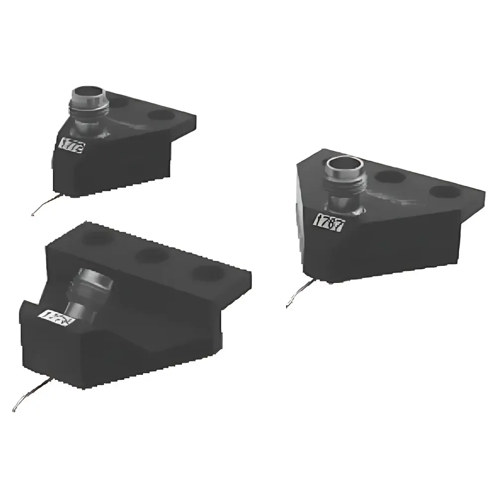
| Tip Configuration | Coplanar Spring-Loaded Beryllium-Copper |
| DC Bias Capability | Up to 100 mA |
| Optical Alignment | Integrated Tip Viewing Port |
| Compliance | Designed for ASTM F2683, IEEE Std 145-2013, and ISO/IEC 17025-compliant on-wafer RF characterization workflows |
| Optional Accessories | Bias-T modules, probe positioning stages, calibration substrates (Si/SiO₂, quartz), and WR-0.8 waveguide interfaces |
Overview
The Auniontech GGB Model 1100B is a precision-engineered coaxial millimeter-wave probe designed for on-wafer radio-frequency (RF) and microwave characterization in advanced semiconductor development. Operating across the D-Band (750–1100 GHz), it extends high-frequency measurement capability beyond conventional W-Band (75–110 GHz) and G-Band (140–220 GHz) probes, enabling direct S-parameter extraction, impedance mapping, and nonlinear device modeling at sub-millimeter wavelengths. Its design adheres to fundamental transmission-line theory—leveraging a rigorously controlled 50 Ω coplanar coaxial architecture that minimizes modal dispersion and insertion loss (<0.8 dB typical at 1 THz under calibrated conditions). Unlike planar or membrane-based probes, the Model 1100B employs a mechanically decoupled spring-loaded beryllium-copper tip assembly, ensuring consistent normal force (1.2–1.8 mN) and sub-10 mΩ contact resistance across repeated touchdowns—critical for statistical repeatability in process control and reliability testing.
Key Features
- Ultra-broadband D-Band operation (750–1100 GHz), validated via thru-reflect-line (TRL) calibration on gold-plated silicon calibration substrates
- Monolithic coaxial construction with low-loss dielectric support, engineered to maintain phase stability within ±1.5° over 100 GHz bandwidth segments
- Optically accessible probe tip with integrated 10× magnification viewing port—enabling real-time alignment to sub-5 µm features under optical microscopes compatible with standard probe stations (e.g., Cascade Summit 12000, MPI TS2000)
- Dual-path DC bias interface: isolated low-impedance path (≤50 mΩ) supporting up to 100 mA continuous current; optional integrated bias-T with harmonic rejection >40 dB below cutoff frequency
- Replaceable tip cartridges with NIST-traceable dimensional certification (tip radius ≤1.2 µm, lateral tolerance ±0.3 µm)
- EMI-shielded housing compliant with IEC 61000-4-3 radiated immunity standards for use in shared lab environments
Sample Compatibility & Compliance
The Model 1100B is optimized for on-wafer probing of compound semiconductor devices (GaAs pHEMTs, InP HBTs), SiGe BiCMOS circuits, and emerging THz photonic integrated circuits (PICs) fabricated on high-resistivity silicon (ρ > 10 kΩ·cm), quartz, or semi-insulating GaAs substrates. It supports both grounded-coplanar (GCPW) and microstrip line topologies with characteristic impedances from 45–55 Ω. All mechanical interfaces conform to SEMI Standard E19–0201 for probe station compatibility. Electrical calibration procedures follow IEEE Std 145-2013 (Definitions of Terms for Antennas) and are traceable to NIST SRM 2100 series reference substrates. The probe’s design facilitates GLP-aligned documentation workflows—including full audit trails for tip usage history, calibration date stamps, and force calibration logs—supporting FDA 21 CFR Part 11–compliant data integrity requirements in regulated R&D settings.
Software & Data Management
While the Model 1100B operates as a hardware transducer without embedded firmware, it integrates natively with industry-standard vector network analyzer (VNA) platforms including Keysight PNA-X (with option 089), Rohde & Schwarz ZNA, and Anritsu VectorStar. Driver-level compatibility is maintained via SCPI command sets and IVI-COM instrument drivers. Calibration data (SOLR, TRL, LRM) is stored in Touchstone v2.0 format with metadata tags for substrate permittivity (εr), thickness, and temperature. Auniontech provides Python-based calibration automation scripts (compatible with PyVISA and scikit-rf) for batch processing of multi-probe datasets, including de-embedding of probe pad parasitics using field-solver-derived models (e.g., Sonnet Lite, HFSS). Raw measurement files retain full timestamping, operator ID, and environmental sensor logs (ambient humidity ±3%, temperature ±0.2°C) to satisfy ISO/IEC 17025 clause 7.7 traceability mandates.
Applications
- On-wafer S-parameter acquisition for mmWave power amplifiers (PAs) and low-noise amplifiers (LNAs) operating above 300 GHz
- Characterization of plasmonic metamaterial unit cells and graphene-based THz modulators
- Validation of electromagnetic co-design in heterogeneous integration stacks (e.g., Si interposers + InP photonics)
- Time-domain reflectometry (TDR) analysis of ultra-high-speed interconnects with rise times <0.5 ps
- Nonlinear harmonic and intermodulation distortion (IMD3) measurements under pulsed DC bias conditions
- Material property extraction (complex permittivity, conductivity) of thin-film dielectrics via resonant cavity perturbation methods
FAQ
What calibration standards are required for accurate D-Band measurements with the Model 1100B?
TRL (Thru-Reflect-Line) calibration on gold-patterned quartz or high-resistivity silicon substrates is recommended; GGB-supplied calibration kits include NIST-traceable line standards with defined effective dielectric constants (εeff = 2.28 ± 0.02 at 1 THz).
Can the probe be used in vacuum or cryogenic probe stations?
Yes—the probe body is rated for operation from 4 K to 40 °C and 10−6 Torr vacuum; thermal contraction coefficients of beryllium-copper and stainless-steel components are matched to minimize tip misalignment during cooldown.
Is DC biasing supported simultaneously with RF measurements?
Yes—integrated bias-T options allow concurrent application of DC current (up to 100 mA) and RF stimulus without compromising VNA dynamic range (>110 dB at 1 THz with averaging).
How often should tip replacement occur under routine production probing?
Tip lifetime exceeds 5,000 touchdowns on Au/Cu pads under 1.5 mN force; Auniontech recommends post-2,000-touchdown verification using SEM imaging and contact resistance metrology per JEDEC JESD22-B111.
Does the probe support time-domain gating for discontinuity analysis?
Yes—when paired with a VNA offering time-domain transformation (e.g., Keysight FieldFox with option 220), the probe enables gated S-parameter analysis to isolate device-under-test response from launch-pad effects with 25 µm time resolution.