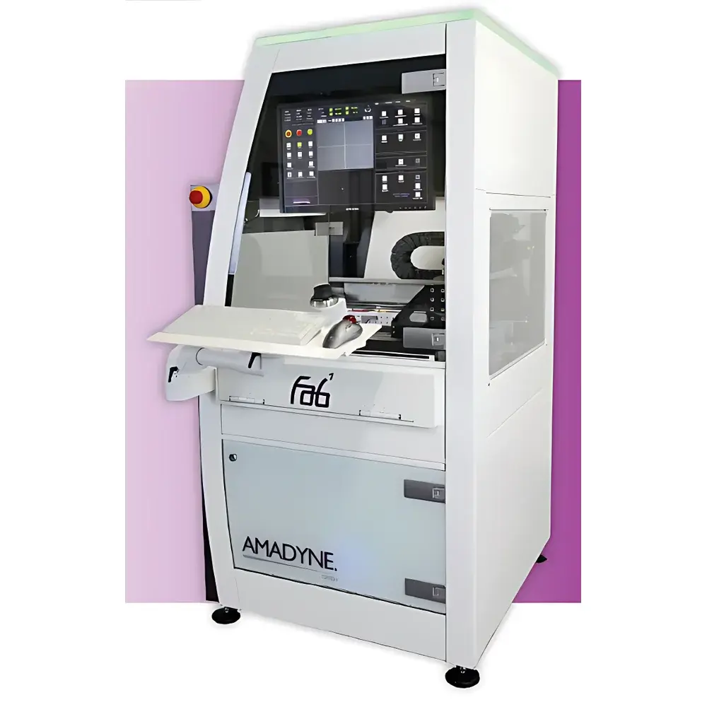
Amadyne Fab1 Automated Die Bonder
| Origin | Germany |
|---|---|
| Manufacturer Type | Authorized Distributor |
| Origin Category | Imported |
| Model | Amadyne Fab1 |
| Pricing | Upon Request |
Overview
The Amadyne Fab1 Automated Die Bonder is a high-precision, modular microassembly platform engineered for semiconductor packaging and advanced heterogeneous integration. Based on a closed-loop vision-guided pick-and-place architecture, the Fab1 employs real-time image processing—leveraging geometric pattern matching (edge, circle, dot, and grayscale correlation)—to achieve sub-micron placement accuracy under controlled inertial and thermal conditions. Designed for R&D labs, pilot lines, and low-to-medium volume production environments, it supports both conventional and next-generation packaging workflows including chip-on-board (COB), multi-chip modules (MCM), flip-chip bonding, eutectic die attach, and adhesive-based assembly. Its compact footprint (<1.2 m²) and rigid steel-aluminum hybrid frame—integrated with embedded vibration-damping castings and iron-core linear motors—ensure mechanical stability critical for repeatable die placement in cleanroom-compatible operation.
Key Features
- Large working envelope: 500 mm × 430 mm XY travel with ±0.5 µm repeatability (typical, calibrated with traceable standards)
- Multi-source component feeding: compatible with waffle trays, gel packs, single 12″ or dual 8″ parallel wafers, and tape-and-reel feeders (including EIA-481-compliant tape carriers)
- Full 360° rotational control of all vacuum nozzles, enabling angular alignment of asymmetric dies and heterogeneously oriented components
- Integrated laminar-flow enclosure with H14 HEPA filtration (99.995% particle capture at 0.3 µm), certified per ISO 14644-1 Class 5
- Linux 4.x-based open software architecture with SQL-backed database backend for full audit trail, recipe management, and process parameter logging
- Modular hardware design supporting field-upgradable configurations—including optional dispensing, flux dipping, eutectic heating, top-view inspection, and post-bond verification modules
- Low power consumption: <500 W nominal operating load; optimized for continuous operation in ISO Class 5–7 cleanrooms
Sample Compatibility & Compliance
The Fab1 accommodates die sizes from 100 µm × 100 µm up to 35 mm × 35 mm, with thicknesses ranging from 50 µm to 1.2 mm. It handles fragile substrates (e.g., GaAs, SiC, glass, LTCC) and temperature-sensitive materials via programmable vacuum pressure control and non-contact nozzle lift-off sequencing. All motion control, vision calibration, and thermal subsystems comply with IEC 61000-6-2 (EMC immunity) and IEC 61000-6-4 (EMC emissions). Software architecture supports 21 CFR Part 11-compliant electronic signatures and audit trails when deployed in GMP-regulated environments. System validation documentation—including IQ/OQ protocols—is available upon request to support GLP/GMP qualification.
Software & Data Management
The graphical user interface (GUI) provides intuitive offline programming with CAD data import (Gerber, ODB++, STEP), wafer map integration (SEMI E142 compliant), and real-time coordinate mapping between camera FOV and stage position. Vision algorithms are trained using reference images captured in situ, with configurable tolerance thresholds for feature detection confidence. Process logs—including placement coordinates, vacuum status, nozzle rotation angle, timestamp, operator ID, and error codes—are stored in structured SQL tables with automated daily backup and role-based access control. Remote diagnostics, firmware updates, and live system monitoring are enabled via secure TLS-encrypted Ethernet connection, supporting predictive maintenance alerts based on motor current profiling and cycle count analytics.
Applications
- R&D prototyping of fan-out wafer-level packaging (FOWLP) and 2.5D/3D IC integration
- Low-volume manufacturing of RF MEMS, photonics assemblies, and high-reliability aerospace sensors
- Thermal interface material (TIM) dispensing and controlled-pressure die attach for power electronics
- Flip-chip pre-alignment prior to thermocompression bonding or reflow
- Post-die-attach optical inspection for void detection, edge chipping, and positional deviation (with optional top-view camera module)
- Process development for Au-Sn, Pb-Sn, and Ag sintering eutectic bonds under nitrogen or formic acid ambient
FAQ
What substrate types and thicknesses can the Fab1 handle?
Standard configuration supports silicon, ceramic, organic laminate, and glass substrates ranging from 0.2 mm to 3.2 mm thick, with custom tooling available for thinner or warped wafers.
Is the system compatible with industry-standard wafer map formats?
Yes—Fab1 natively imports SEMI E142-compliant wafer map files (.csv, .xml) and supports die-level binning data for selective pickup logic.
Can the software generate compliance reports for quality audits?
All process logs include ISO/IEC 17025-aligned metadata (timestamp, operator, equipment ID, environmental sensor readings); exportable as PDF or CSV with digital signature capability.
What level of technical support is provided after installation?
Amadyne-certified engineers deliver on-site commissioning, operator training, and annual preventive maintenance; remote support includes screen-sharing diagnostics and firmware version management.
Are safety interlocks and emergency stop functions certified to international standards?
Yes—the system meets CE Machinery Directive 2006/42/EC and ISO 13857 requirements, with dual-channel monitored E-stop circuitry and light curtain integration capability.
Related Products


