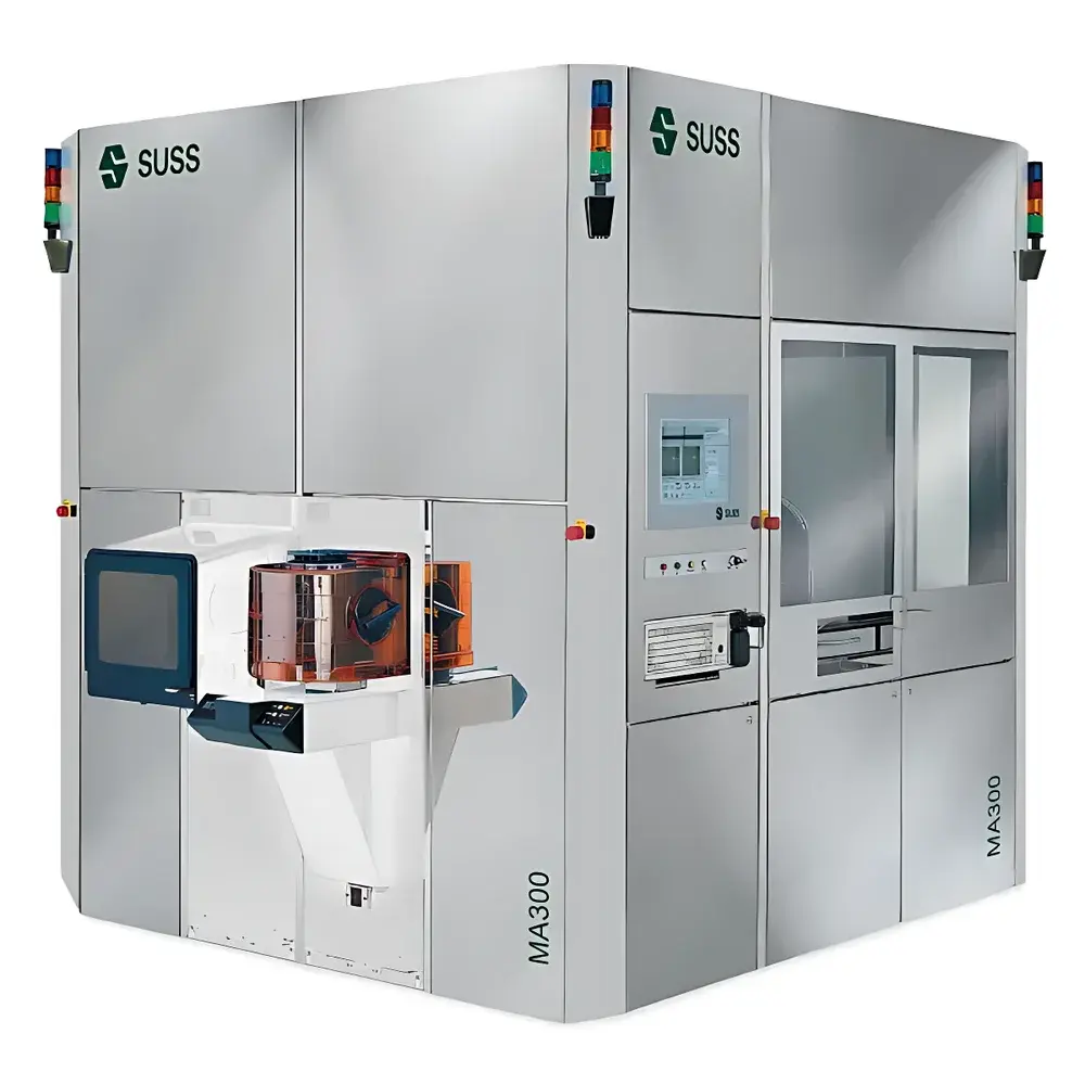
SUSS MA300 Gen3 Fully Automated Mask Aligner
| Brand | SUSS MicroTec |
|---|---|
| Origin | Germany |
| Model | MA300 Gen3 |
| Wafer Size Support | 200 mm & 300 mm |
| Alignment Accuracy (Top-Side) | ±0.5 µm |
| Alignment Modes | Top-Side, Bottom-Side, Infrared (IR) |
| Exposure Method | Contact/Near-Contact Photolithography |
| Optical System | MO Exposure Optics® |
| Application Focus | Advanced Packaging (TSV, RDL, Bumping), MEMS, LED, Power Devices, WLP, Flip-Chip |
| Compliance | Designed for ISO Class 5–7 cleanroom integration |
| Automation Level | Full cassette-to-cassette robotic handling |
Overview
The SUSS MA300 Gen3 Fully Automated Mask Aligner is a high-precision, production-grade photolithography platform engineered for contact and near-contact exposure of 200 mm and 300 mm wafers in advanced semiconductor packaging and microfabrication environments. Unlike projection-based steppers or scanners, the MA300 Gen3 leverages proven proximity lithography—where the photomask is positioned at a precisely controlled gap (typically 10–50 µm) above the resist-coated wafer—to achieve sub-micron pattern transfer without depth-of-field constraints. This principle enables robust, high-fidelity imaging through thick photoresists (>100 µm), making it indispensable for through-silicon via (TSV), redistribution layer (RDL), and bump lithography processes where conventional optical projection systems face resolution or focus limitations. Built on over four decades of SUSS MicroTec’s mask aligner heritage, the Gen3 platform integrates mechanical stability, thermal management, and vibration isolation to ensure long-term repeatability across extended production runs and multi-user R&D facilities.
Key Features
- DirectAlign® Top-Side Alignment: Achieves ≤ ±0.5 µm overlay accuracy using real-time image correlation and SUSS’ proprietary structure detection algorithm—validated per SEMI S2/S8 safety and performance guidelines.
- MO Exposure Optics®: A high-uniformity, broadband (i-line, g-line, h-line) illumination system with integrated dose control and intensity homogenization, delivering <±2% dose uniformity across full 300 mm wafers.
- Multi-Mode Alignment Architecture: Supports top-side, bottom-side, and infrared (IR) alignment—enabling precise registration on thinned wafers (<50 µm), opaque substrates (e.g., SiC, GaN), and double-sided patterned wafers without manual repositioning.
- Thick-Resist Process Capability: Optimized gap control and vacuum chuck design accommodate photoresist thicknesses from 1 µm to >200 µm while maintaining consistent proximity gap and minimizing mask damage risk.
- Fully Automated Workflow: Integrated robotic handler with SECS/GEM interface, dual-loadports, and SMIF-compatible cassette stations support unattended operation in 24/7 fab environments.
- Modular Cleanroom Integration: Designed for ISO Class 5–7 cleanroom deployment with HEPA-filtered internal environment, particle monitoring ports, and ESD-safe construction per ANSI/ESD S20.20.
Sample Compatibility & Compliance
The MA300 Gen3 accommodates standard silicon, compound semiconductor (GaAs, SiC, GaN), glass, and ceramic substrates up to 300 mm diameter and 1.5 mm thickness. Its IR alignment module supports alignment through substrates with transmission >10% at 1000–1600 nm—critical for processed wafers with metal layers or embedded interposers. The system complies with CE machinery directive 2006/42/EC, IEC 61000-6-2/6-4 EMC standards, and includes full documentation packages for IQ/OQ validation under GMP and ISO 9001 frameworks. Optional audit trail logging and electronic signature modules meet FDA 21 CFR Part 11 requirements for regulated packaging development labs.
Software & Data Management
Controlled via SUSS’ proprietary MA-OS (Mask Aligner Operating System), the platform provides deterministic recipe management, real-time process parameter logging (gap, dose, alignment error vectors, vacuum level), and CSV/PDF export for traceability. All alignment data—including fiducial recognition confidence scores and stage position residuals—are timestamped and stored with user ID attribution. The system supports remote diagnostics via secure TLS-encrypted connection and integrates with factory MES via standardized SECS/GEM HSMS protocols. Audit trail functionality records all critical parameter changes, user logins, and exposure events with immutable timestamps—fully compliant with GLP and internal quality system requirements.
Applications
The MA300 Gen3 serves as a foundational lithography tool in advanced packaging lines for TSV formation, fan-out wafer-level packaging (FOWLP), and copper pillar bumping. It is equally deployed in MEMS foundries for inertial sensor and pressure transducer fabrication, in LED manufacturing for phosphor patterning and chip-scale packaging, and in power device fabs for gate trench and passivation layer definition. Its flexibility extends to university cleanrooms and industrial R&D centers conducting process development for heterogeneous integration, hybrid bonding, and 3D IC prototyping—where rapid iteration, low cost-per-exposure, and compatibility with non-standard substrates are essential.
FAQ
What wafer sizes does the MA300 Gen3 support?
It handles 200 mm and 300 mm wafers with optional adaptability for 150 mm via software-configurable stage limits.
Can the system perform alignment on thinned or opaque substrates?
Yes—via its integrated infrared (IR) alignment mode, which operates at wavelengths penetrating silicon up to ~750 µm thickness and common metallization layers.
Is the MA300 Gen3 compatible with thick photoresists used in TSV applications?
Yes—the system is optimized for resist thicknesses ranging from 1 µm to over 200 µm, with programmable gap control and force-limited contact modes to prevent mask damage.
Does the platform support regulatory compliance for medical or aerospace packaging development?
With optional 21 CFR Part 11-compliant software modules and full IQ/OQ documentation, it meets traceability and audit readiness requirements for regulated environments.
How is process reproducibility ensured across shifts and operators?
Through automated recipe locking, hardware-calibrated alignment reference points, and built-in daily verification routines that validate alignment accuracy, dose uniformity, and gap repeatability before production starts.


