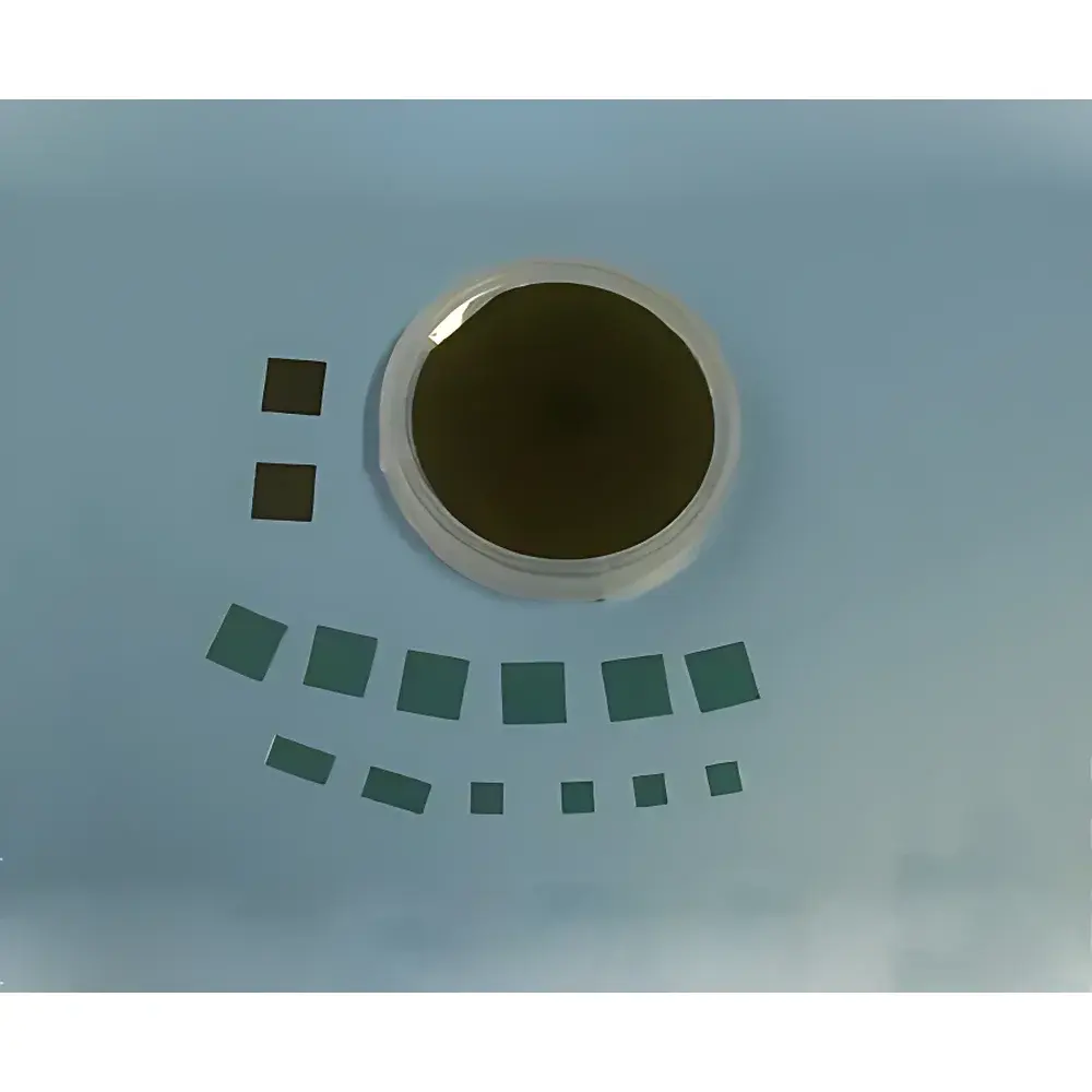
合肥科晶 4H-SiC Epitaxial Wafer: P-Type 4H-SiC Thin Film on 4H-SiC Substrate
| Brand | Hefei Kejing |
|---|---|
| Origin | USA |
| Manufacturer Type | Authorized Distributor |
| Origin Category | Imported |
| Model | 4H-SiC Epitaxial Film on 4H-SiC Substrate, P-Type |
| Diameter | 100 mm ±0.5 mm |
| Thickness | 525 µm ±25 µm |
| Epilayer Thickness | 4.3 µm ±10% |
| Epilayer Doping Concentration | 1.4×10¹⁷ cm⁻³ (−30%/+0%) |
| Carrier Concentration | (3–10)×10¹⁶ cm⁻³ |
| Conductivity Type | P-type |
| Surface Finish | Double-Side CMP Polished (Si-face polished only) |
| Substrate Orientation | <0001>, 8.0° ±0.5° off-axis toward (10-10) |
| Off-Orientation (OF) Length | 15.9 mm ±1.7 mm |
| Flat Orientation | 90° clockwise from OF ±5° |
| IF Length | 8.0 mm ±1.7 mm |
| Substrate Resistivity | <0.03 Ω·cm |
| Edge Exclusion | 1 mm |
| Packaging | Class 1000 Cleanroom, Class 100 Bag Vacuum-Sealed or Single-Wafer Cassette |
Overview
The Hefei Kejing 4H-SiC Epitaxial Wafer — P-Type 4H-SiC Thin Film on 4H-SiC Substrate — is a high-purity, homoepitaxial semiconductor structure engineered for advanced power electronics, high-temperature sensors, and radiation-hardened device fabrication. This wafer leverages chemical vapor deposition (CVD) epitaxy to grow a precisely doped 4H polytype silicon carbide film on a crystalline 4H-SiC substrate, ensuring atomic-level lattice matching and minimal interfacial defect density. The crystallographic orientation with controlled 8.0° off-cut enables optimal step-flow growth kinetics and uniform dopant incorporation across the epilayer. Designed for integration into high-voltage (>1.2 kV), high-frequency (>100 kHz), and high-thermal-conductivity (>3.7 W/cm·K) platforms, this material meets stringent requirements for vertical power diodes (e.g., PiN, Schottky barrier), MOSFETs, and JFETs operating under extreme thermal and electrical stress.
Key Features
- Homoepitaxial architecture: Identical 4H-SiC polytype in both substrate and epilayer minimizes threading dislocation density (<1 × 10⁴ cm⁻² typical) and eliminates interfacial strain-induced defects.
- P-type doping via aluminum (Al) or boron (B) precursors, calibrated to achieve carrier concentrations within (3–10) × 10¹⁶ cm⁻³ — optimized for gate-controlled conduction and low specific on-resistance (Ron,sp) in vertical devices.
- Double-side chemical-mechanical polishing (CMP): Si-face polished to ≤0.2 nm RMS roughness; C-face left as-received or optionally polished per customer specification.
- Tight dimensional tolerances: 100 mm diameter ±0.5 mm, thickness 525 µm ±25 µm, epilayer thickness 4.3 µm ±10%, enabling compatibility with standard 4-inch semiconductor processing tools (lithography, etching, metallization).
- Controlled off-axis geometry: 8.0° ±0.5° miscut toward (10-10) ensures stable step-terrace growth mode and suppresses Si droplet formation during high-temperature epitaxy.
Sample Compatibility & Compliance
This epitaxial wafer is fully compatible with industry-standard front-end semiconductor processes including photolithography (i-line, KrF), dry etching (ICP-RIE with Cl₂/BCl₃ chemistries), and high-temperature metallization (Ti/Al/Ni/Au, Ni/Ti/Al). It conforms to SEMI MF1530 specifications for SiC wafer flatness (TTV < 2 µm), warp (< 15 µm), and bow (< 10 µm). All wafers undergo post-CMP inspection per SEMI F61 and are certified for use in ISO 14644-1 Class 5 (ISO Class 5) cleanroom environments. Traceability includes full lot-level documentation of growth conditions, secondary ion mass spectrometry (SIMS) dopant profiling, and Hall-effect mobility characterization — supporting GLP-compliant R&D and qualification testing per JEDEC JESD22-A108 and AEC-Q101 standards.
Software & Data Management
While this is a passive substrate product (no embedded firmware or onboard software), full metrology data packages are provided digitally upon shipment. These include: (1) SIMS depth profiles for Al/B dopant distribution and background impurities (N, V, Fe); (2) Hall-effect measurement reports (carrier concentration, mobility, resistivity at 300 K and 500 K); (3) X-ray diffraction (XRD) rocking curve FWHM data for epilayer crystallinity; (4) atomic force microscopy (AFM) surface topography maps; and (5) optical microscopy defect maps (particles, pits, scratches). Data files comply with ASTM E2053-20 metadata standards and are delivered in CSV, PDF, and TIFF formats. Secure cloud access (via password-protected portal) supports audit-ready data retention for FDA 21 CFR Part 11–aligned quality systems.
Applications
- High-voltage power switching devices: PiN diodes, trench-gate MOSFETs, and cascode JFETs requiring low forward voltage drop and fast recovery characteristics.
- Radiation-tolerant microelectronics: Space-grade DC-DC converters, nuclear reactor monitoring sensors, and particle detector substrates.
- High-temperature electronics: Downhole oil/gas instrumentation, jet engine control modules, and combustion chamber feedback sensors (operable up to 600 °C junction temperature).
- Quantum sensing platforms: Nitrogen-vacancy (NV) center hosting layers for magnetometry and thermometry applications leveraging SiC’s wide bandgap and spin coherence properties.
- Research-grade heterostructure development: Template for subsequent GaN-on-SiC or AlN-on-SiC growth where lattice-matched nucleation is critical.
FAQ
What is the maximum allowable thermal budget for post-epitaxial processing without degrading the P-type dopant profile?
Thermal treatments above 1600 °C in inert or reducing atmospheres may induce dopant diffusion or compensation. For process stability, keep annealing below 1500 °C for ≤10 minutes.
Is the C-face of the substrate available with optional polishing?
Yes — double-side polishing (Si-face + C-face) is available as a custom option; minimum order quantity applies.
Do you provide cross-sectional TEM samples or cleaved bevels for interface analysis?
Upon request and NDA execution, representative cross-section TEM lamellae or mechanical bevels can be supplied with EDS mapping support.
Can this wafer be used for fabricating normally-off enhancement-mode devices?
Not directly — P-type epilayers are typically used for anode regions or body layers. Enhancement-mode operation requires n-channel structures; complementary N-type variants are available under separate model numbers.
What packaging certifications accompany each shipment?
Each wafer ships in a Class 100 vacuum-sealed bag inside a rigid Class 1000 cleanroom cassette, accompanied by a Certificate of Conformance (CoC) and traceable lot ID label compliant with ISO 9001:2015 documentation protocols.
Related Products

 and Vehicle Classification System")