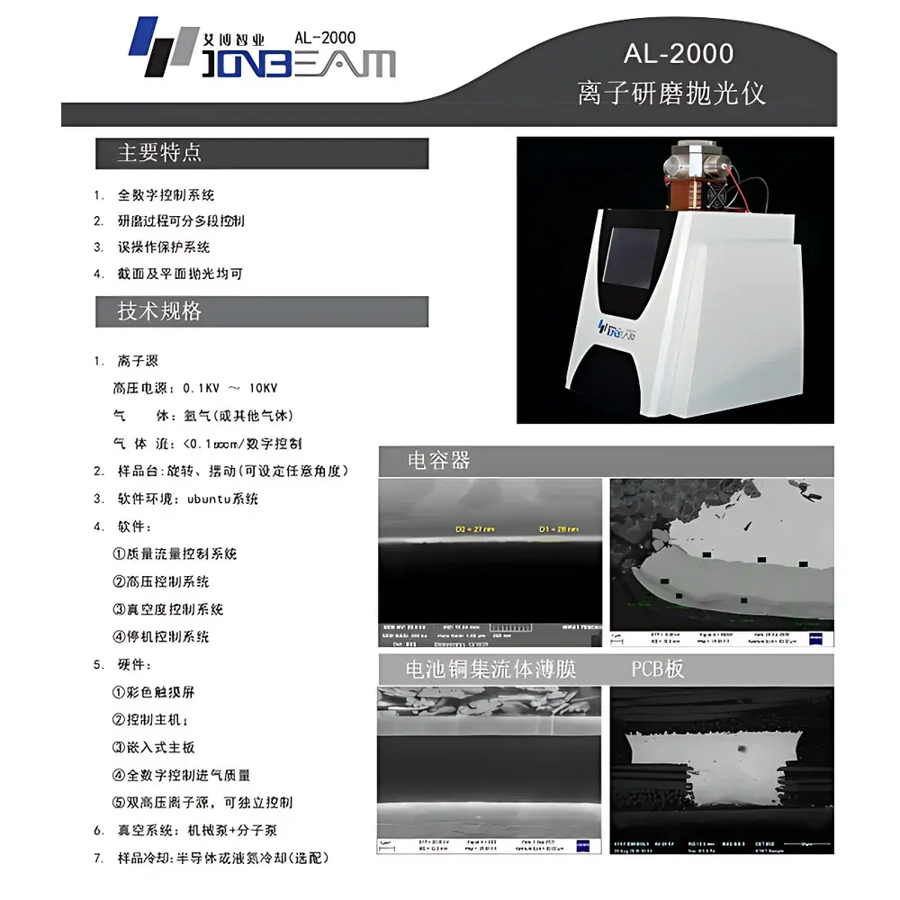
Abbe AL-2000 Ion Beam Milling System (Cross-section, Polishing & Etching)
| Brand | Abbe / Ionbeam |
|---|---|
| Origin | Beijing, China |
| Manufacturer Type | OEM Manufacturer |
| Region Category | Domestic (China) |
| Model | AL-2000 |
| Pricing | Upon Request |
| Sample Diameter Capacity | Ø0–25 mm |
| Ultimate Vacuum | 5 × 10⁻³ Pa (without Ar gas) |
| Acceleration Voltage Range | 200–10,000 V |
Overview
The Abbe AL-2000 Ion Beam Milling System is an integrated, high-precision ion beam sample preparation instrument engineered for the controlled removal of material from solid specimens using focused inert-gas ion bombardment—primarily argon ions accelerated under high-voltage DC fields. Operating on the principle of physical sputtering, the system delivers directional, low-damage milling essential for preparing electron-transparent thin sections, artifact-free cross-sections, and atomically smooth surfaces for transmission electron microscopy (TEM), scanning electron microscopy (SEM), electron backscatter diffraction (EBSD), and focused ion beam (FIB)-complementary workflows. Unlike thermal or mechanical polishing methods, ion beam milling avoids plastic deformation, phase transformation, or localized heating—making it especially suitable for temperature-sensitive materials including polymer films, multilayer thin-film stacks, organic-inorganic hybrids, and brittle intermetallic compounds. The AL-2000 is purpose-built for laboratories requiring reproducible, operator-independent preparation of high-fidelity samples in compliance with TEM/SEM specimen standards defined by ASTM E1558 and ISO/IEC 17025-accredited workflows.
Key Features
- Dual independently controllable ion guns enable asymmetric milling, differential rate control, and simultaneous top/bottom surface irradiation—critical for minimizing shadowing effects and achieving uniform thickness across large-area samples (up to Ø25 mm).
- Motorized rotating sample stage ensures continuous angular variation during milling, significantly improving surface uniformity and reducing preferential sputtering artifacts.
- Digital automated control system supports programmable voltage ramping, timed dwell sequences, and energy-step profiling—allowing single-sample processing with dynamically adjusted acceleration voltage (200–10,000 V) to accommodate layered structures with varying sputter yields.
- Dedicated cross-section sample holder with precision tilt alignment facilitates accurate edge-on milling of interfaces, grain boundaries, and device heterostructures—compatible with standard SEM stubs and TEM half-grids.
- Integrated beam shield and adjustable collimating apertures minimize stray ion exposure, protecting non-target regions and preserving native surface chemistry prior to analysis.
- Optional Peltier-based semiconductor cooling stage maintains sample temperature below 10 °C during extended milling—reducing thermal drift, inhibiting polymer chain mobility, and suppressing recrystallization in metastable phases.
- Self-diagnostic vacuum interlock and over-pressure protection ensure stable operation at ultimate vacuum levels ≤5 × 10⁻³ Pa (base pressure, no Ar flow), meeting minimum requirements for contamination-sensitive TEM lamellae preparation.
Sample Compatibility & Compliance
The AL-2000 accommodates a broad spectrum of inorganic, organic, and composite materials—including but not limited to Si/SiO₂ wafers, perovskite photovoltaic layers, battery electrode composites (NMC, LFP), metallic alloys (Al, Ti, Ni-based superalloys), geological thin sections, and cryo-stabilized biological tissues embedded in resin. Its low-energy ion capability (5 keV) support rapid bulk removal for initial thinning. All operational parameters are logged with timestamped metadata, supporting audit-ready documentation per GLP and GMP environments. The system’s vacuum architecture and gas handling design conform to ISO 27427 (vacuum equipment safety) and are compatible with inert-gas purging protocols required for oxygen-sensitive samples.
Software & Data Management
The AL-2000 runs on a Windows-based control interface featuring real-time ion current monitoring, stage position feedback, vacuum status visualization, and recipe-driven automation. Each milling protocol is stored as a version-controlled XML file containing voltage profiles, rotation speed, gas flow setpoints (when Ar is introduced), and duration per segment. Audit trails record all user actions, parameter changes, and system alarms—fully compliant with FDA 21 CFR Part 11 requirements when deployed with electronic signature modules and network authentication. Exportable CSV logs integrate seamlessly with laboratory information management systems (LIMS) and digital microscopy platforms such as Thermo Fisher Scientific’s Velox or JEOL’s JSM software suites.
Applications
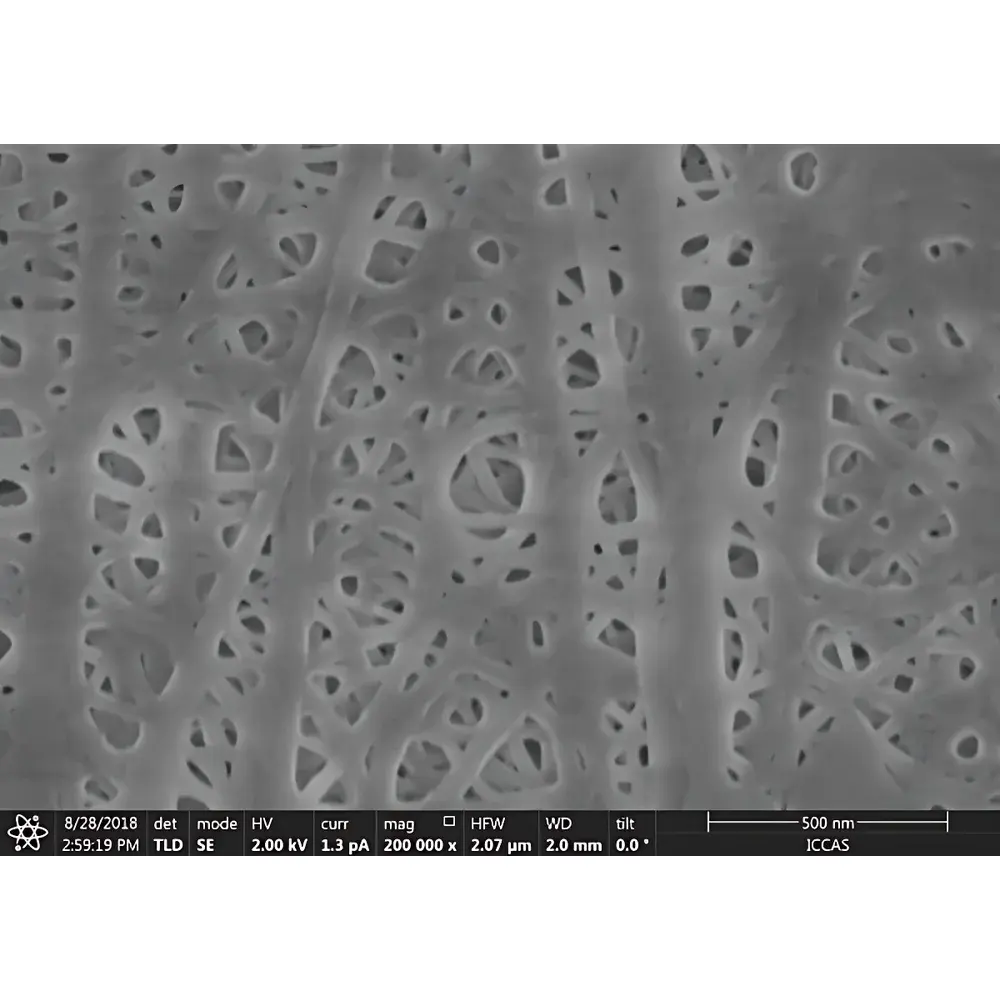
- Preparation of electron-transparent lamellae for TEM analysis of nanoscale defects, dislocation networks, and interfacial segregation.
- Cross-sectional milling of microelectronic devices (e.g., FinFETs, 3D NAND stacks) to expose buried metallization layers and dielectric interfaces without delamination.
- Surface polishing of EBSD samples to eliminate mechanical deformation layers and reveal true crystallographic orientation contrast.
- Ion etching of maskless pattern transfer for soft lithography templates and MEMS structural release.
- In-situ plasma cleaning of specimen surfaces prior to coating or high-resolution imaging—eliminating hydrocarbon contamination without UV/ozone exposure.
FAQ
What vacuum level is required for optimal ion beam stability and minimal contamination?
The AL-2000 achieves stable beam operation at ≤5 × 10⁻³ Pa base pressure; introduction of argon gas during milling typically raises operating pressure to 1–5 × 10⁻¹ Pa, within the optimal range for Ar⁺ sputtering efficiency.
Can the system prepare site-specific cross-sections without FIB assistance?
Yes—the dedicated cross-section holder enables precise mechanical alignment of pre-defined regions of interest (ROIs); combined with dual-gun asymmetry control, it supports targeted milling of features down to ~5 µm lateral resolution without FIB pre-milling.
Is semiconductor cooling necessary for all sample types?
Cooling is recommended for polymers, frozen-hydrated resins, and low-melting-point alloys to suppress thermal diffusion and surface roughening; it is optional but strongly advised for quantitative EBSD or low-k dielectric analysis.
How does the AL-2000 ensure repeatability between operators and sessions?
Through full digital parameter locking, stage homing routines, and automated recipe recall—eliminating manual adjustments and enabling identical milling conditions across shifts, instruments, and multi-site laboratories.


