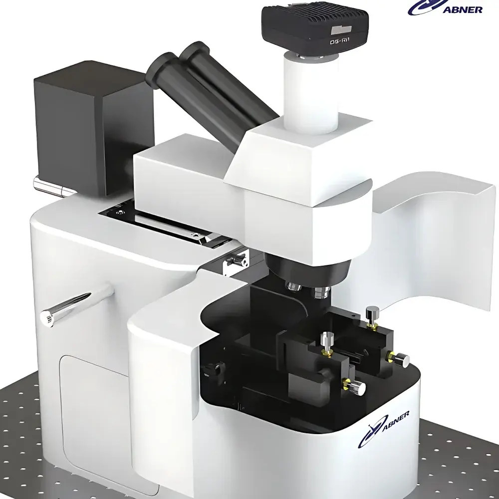
Abner ABN-AFM-001 Atomic Force Microscope
| Brand | Abner |
|---|---|
| Origin | Jiangsu, China |
| Model | ABN-AFM-001 |
| Instrument Type | Material-oriented AFM |
| Sample Dimensions | Max 15 mm × 15 mm × 2 mm |
| Scan Range | 70 µm × 70 µm (X–Y), 17 µm (Z) |
| Lateral Resolution | ≤1 nm |
| Vertical Resolution | ≤0.1 nm |
| XY Noise | ≤0.01 nm RMS |
| Z Noise | ≤0.05 nm RMS |
| Scan Speed | Up to 10 Hz |
| Probe Compatibility | Si probes with spring constants from 0.01 N/m to 40 N/m |
| Scanner | High-precision closed-loop piezoelectric scanner |
| Environmental Requirements | 18–25 °C, ≤60% RH |
| Image Resolution | 512×512 to 2048×2048 pixels |
| Interface | USB and Ethernet |
| Power Supply | 220 V/50 Hz or 110 V/60 Hz |
Overview
The Abner ABN-AFM-001 Atomic Force Microscope is a precision-engineered scanning probe instrument designed for nanoscale surface topography and mechanical property characterization under ambient and optional liquid environments. Operating on the principle of detecting van der Waals and short-range interatomic forces via a microfabricated cantilever probe, the ABN-AFM-001 delivers sub-nanometer vertical resolution (≤0.1 nm RMS) and lateral resolution down to ≤1 nm—enabling quantitative analysis of surface morphology, step heights, roughness, and local mechanical responses. Its closed-loop piezoelectric scanner ensures high positional fidelity and repeatability across repeated scans, critical for comparative metrology in materials development and process validation. The system supports three primary operational modes—contact, tapping (intermittent contact), and non-contact—allowing adaptive selection based on sample compliance, adhesion, and environmental constraints. This flexibility makes it suitable for rigid inorganic substrates (e.g., silicon wafers, sapphire), soft polymeric films, biological specimens (fixed or hydrated), and functional thin-film architectures.
Key Features
- Nanometer-scale lateral resolution and sub-angstrom vertical resolution, verified per ISO 25178-6 and ASTM E2492 standards for surface texture metrology.
- Closed-loop piezoelectric scanning head with real-time position feedback, minimizing hysteresis and thermal drift during extended acquisitions.
- Multi-mode operation: Contact mode for high-resolution imaging of robust samples; tapping mode for reduced tip–sample interaction force (ideal for soft, adhesive, or heterogeneous surfaces); non-contact mode for ultra-low-force imaging in air or controlled gaseous environments.
- Low-noise detection architecture: XY noise ≤0.01 nm RMS, Z noise ≤0.05 nm RMS—optimized for high-fidelity measurement of atomic steps, monolayer thickness variations, and subtle surface corrugations.
- Modular probe compatibility: Supports standard silicon cantilevers with tunable spring constants (0.01–40 N/m), enabling customization for stiffness mapping, force spectroscopy, or high-speed dynamics.
- Flexible sample handling: Accommodates specimens up to 15 mm × 15 mm × 2 mm; compatible with standard TEM grids, silicon chips, glass coverslips, and custom liquid cells for in situ aqueous measurements.
Sample Compatibility & Compliance
The ABN-AFM-001 is validated for use with solid, thin-film, and liquid-immersed samples—including conductive and insulating substrates, 2D materials (graphene, TMDs), polymer blends, biological membranes, and electrochemical interfaces. It meets general laboratory safety requirements per IEC 61010-1 and electromagnetic compatibility (EMC) directives (EN 61326-1). While not certified for GLP/GMP-regulated production environments out-of-the-box, its data acquisition logs include timestamped metadata, user ID tagging, and raw channel export—supporting audit readiness for ISO/IEC 17025-accredited testing laboratories. Optional firmware upgrades enable 21 CFR Part 11-compliant electronic signatures and audit trails for regulated life science applications.
Software & Data Management
The instrument is operated via a native Windows-based GUI featuring intuitive workflow navigation, real-time image preview, and synchronized multi-channel acquisition (topography, phase, amplitude, deflection). All images are saved in vendor-neutral formats (e.g., .tif with embedded metadata, .csv for height profiles) to ensure interoperability with third-party analysis platforms such as Gwyddion, MountainsSPIP, and MATLAB. Batch processing scripts support automated roughness calculation (Sa, Sq, Sz per ISO 25178-2), grain analysis, and cross-sectional profiling. Data integrity is reinforced through checksum-verified file writes and optional network-attached storage (NAS) integration via Ethernet interface.
Applications
- Materials Science: Quantitative roughness mapping of CVD-grown graphene, layer-counting of transition metal dichalcogenides (MoS₂, WSe₂), and defect density assessment in ALD-deposited dielectrics.
- Semiconductor Metrology: Wafer-level inspection of CMP-induced scratches, trench profile analysis in FinFET structures, and post-etch residue characterization.
- Life Sciences: Nanomechanical mapping of cell membrane elasticity (Young’s modulus), conformational analysis of immobilized proteins, and time-lapse imaging of lipid bilayer reorganization in buffer.
- Energy Materials: Surface homogeneity evaluation of perovskite photovoltaic layers, pore structure quantification in battery separator membranes, and catalyst nanoparticle dispersion analysis.
- Academic Research & Education: Pedagogical demonstration of tip–sample interaction physics, hands-on training in SPM calibration protocols, and undergraduate thesis projects in surface science and nanomechanics.
FAQ
What scanning modes does the ABN-AFM-001 support?
Contact, tapping (intermittent contact), and non-contact modes—all accessible via software-selectable feedback control parameters.
Can the system perform force spectroscopy or nanomechanical mapping?
Yes—the closed-loop scanner and calibrated cantilever library enable quantitative force–distance curve acquisition and elastic modulus extraction using Hertz or Sneddon models.
Is liquid-phase imaging supported?
Yes—compatible with commercially available fluid cells; requires optional liquid-stage mounting kit and vibration-isolated optical table for stable operation.
What is the maximum scan area and Z-range?
70 µm × 70 µm in XY; 17 µm in Z—expandable via motorized stage option for large-area stitching.
Does the system comply with regulatory data integrity standards?
Raw data export and metadata logging meet baseline requirements for ISO/IEC 17025; 21 CFR Part 11 compliance achievable via optional validated software module and procedural controls.


