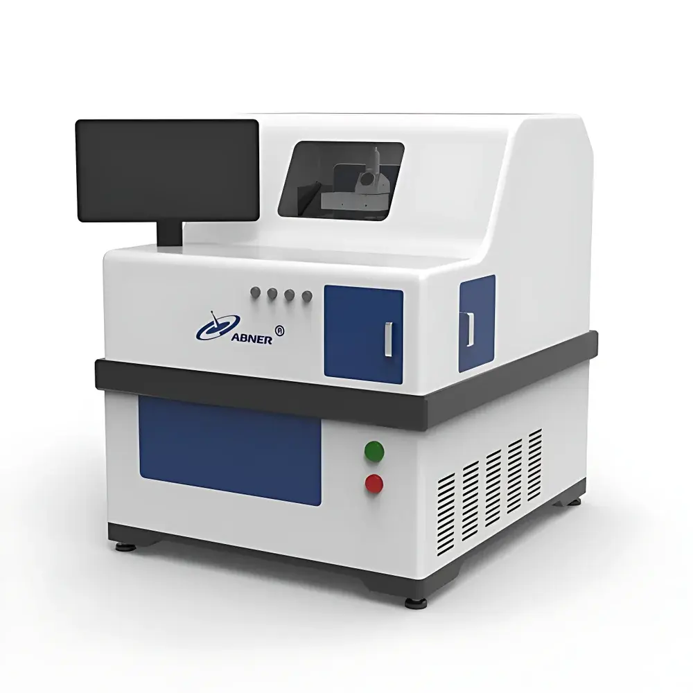
Abner ABN-PRO-002 Fully Automated Wafer Probe Station
| Brand | Abner |
|---|---|
| Origin | Jiangsu, China |
| Model | ABN-PRO-002 |
| Operation Type | Fully Automatic |
| Probe Positioning Resolution | 1 µm |
| Integrated Vacuum Pump | Yes |
| Display | 27-inch 2K Full HD Monitor |
| Motorized Axes | X-Y-Z with Sample Stage Heating & Vacuum Chuck Control |
| Optical Imaging | Nikon CCD Camera (Visible to Near-IR) |
| RF Connectivity | Supported with Multiple RF Connector Types (SMA, K, V) |
| Probe Compatibility | GGB (USA), Korean OEM, and Domestic Probes |
| External Instrument Integration | Picosecond/Femtosecond Lasers, Raman, SHG, Photoconductivity Systems |
Overview
The Abner ABN-PRO-002 Fully Automated Wafer Probe Station is an engineered platform for high-precision electrical and optoelectronic characterization of semiconductor wafers up to 300 mm in diameter. Built upon a rigid, vibration-damped granite base and sealed cleanroom-compatible enclosure, the system implements a closed-loop motorized XYZ stage architecture with sub-micron repeatability—enabling reliable contact formation between microfabricated probes and device pads under controlled thermal and vacuum conditions. Its core measurement paradigm supports DC/RF parametric testing, transient photocurrent mapping, and synchronized optical stimulation (e.g., laser-induced carrier injection), making it suitable for R&D labs validating advanced node ICs, power devices, MEMS, and emerging photonic integrated circuits (PICs). The station operates within Class 1000 cleanroom environments and is designed to meet mechanical stability requirements outlined in SEMI F47 and ISO 14644-1.
Key Features
- Sub-micron probe positioning accuracy: 1 µm resolution across all three translational axes, achieved via stepper-motor-driven linear stages with integrated encoders and real-time position feedback.
- Integrated thermal control: Motorized sample stage with programmable heating (up to 150 °C) and active cooling options, compatible with temperature-dependent parameter extraction per JEDEC JESD51 standards.
- Vacuum-assisted wafer handling: Onboard oil-free vacuum pump supporting chuck pressure regulation from 0.1 to 80 kPa, ensuring uniform adhesion across full 300 mm wafers without edge lift or drift.
- Optical alignment subsystem: High-magnification stereomicroscope coupled with Nikon CCD camera covering 400–1700 nm spectral range, enabling simultaneous visual confirmation of probe tip geometry, pad alignment, and laser spot placement.
- RF-ready interface architecture: Pre-routed coaxial pathways with SMA, K, and V-type RF connectors; impedance-matched cabling paths minimize signal loss and phase distortion up to 67 GHz.
- Modular probe compatibility: Standardized probe holder design accepts industry-standard cantilever and wedge probes—including GGB (USA), Korean OEM, and domestic variants—without mechanical adaptation.
Sample Compatibility & Compliance
The ABN-PRO-002 accommodates bare silicon, SOI, GaN-on-Si, SiC, and compound semiconductor wafers (2″, 4″, 6″, 8″, and 12″) with standard thicknesses (275–775 µm). Chuck flatness tolerance is maintained at ≤2 µm over 300 mm span. All internal surfaces are electrostatically dissipative (10⁶–10⁹ Ω/sq), conforming to ANSI/ESD S20.20. Mechanical interfaces comply with SEMI E10 (Specification for Definition and Measurement of Equipment Reliability and Maintainability) and support integration into automated test equipment (ATE) workflows via SECS/GEM protocol adapters (optional). System documentation includes traceable calibration records aligned with ISO/IEC 17025 requirements for metrological assurance.
Software & Data Management
Control is executed via Abner’s proprietary ProbeStation Control Suite (PSCS v3.2), a Windows-based application supporting scriptable test sequencing (Python API), multi-channel I-V/C-V acquisition synchronization, and time-stamped event logging. Raw data export follows HDF5 format with embedded metadata (timestamp, stage coordinates, temperature, vacuum level, optical gain settings). Audit trail functionality satisfies FDA 21 CFR Part 11 requirements for electronic records and signatures, including user-level access control, immutable log history, and change tracking for all configuration parameters. Integration with Keysight PathWave, Tektronix ATE platforms, and LabVIEW is supported through standardized IVI drivers.
Applications
- Parametric testing of FinFET, GAA, and nanosheet transistors during process development.
- DC and pulsed IV characterization of wide-bandgap power devices (SiC MOSFETs, GaN HEMTs) under variable temperature and bias stress.
- Optoelectronic device validation: responsivity mapping of photodiodes, quantum dot arrays, and plasmonic sensors using synchronized laser excitation and lock-in detection.
- Non-destructive failure analysis: Raman spectroscopy and second-harmonic generation (SHG) imaging of strain distribution and crystal defects in epitaxial layers.
- Reliability assessment: TDDB, HCI, and NBTI stress testing with real-time leakage monitoring and automated probe repositioning after thermal cycling.
FAQ
Does the ABN-PRO-002 support automated wafer loading?
Yes—it is compatible with third-party front-end loaders (FEL) via SMIF/FOUP interface modules; fully integrated auto-load capability requires optional robotic handler add-on.
Can the system perform RF S-parameter measurements?
Yes, when paired with a vector network analyzer (VNA); the station provides calibrated RF launch points, ground-signal-ground (GSG) probe alignment fixtures, and de-embedding support for on-wafer calibration kits (e.g., TRL, LRM).
Is thermal calibration traceable to national standards?
All temperature sensors are factory-calibrated against NIST-traceable references; calibration certificates include uncertainty budgets per ISO/IEC 17025 Annex A.
What safety certifications does the system hold?
CE marking (EN 61000-6-2/6-4, EN 61010-1), UL 61010-1 recognition, and RoHS 3 compliance are documented in the technical file supplied with each unit.
How is software validation handled for regulated environments?
PSCS v3.2 includes IQ/OQ documentation templates, installation verification checklists, and performance qualification protocols aligned with ASTM E2500 and GAMP5 guidelines.


