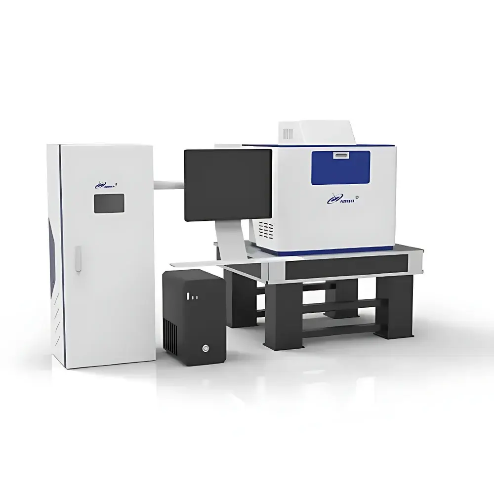
Abner ABN-WAFER-001 Fully Automated Wafer-Level Transfer Stage
| Brand | Abner |
|---|---|
| Origin | Jiangsu, China |
| Manufacturer Type | Authorized Distributor |
| Product Category | Domestic |
| Model | ABN-WAFER-001 |
| Price | USD 35,000 (FOB Jiangsu) |
| Product Type | Motorized Translation Stage |
| Travel Range (X/Y) | ±25 mm |
| Positioning Accuracy | ≤ 0.1 mm |
| Step Resolution | ≤ 2 µm |
| Max Load | 4 kg |
| Z-Axis Height Adjustment | 0–160 mm |
| Vacuum Adsorption | Uniform Negative Pressure |
| Compatible Wafer Sizes | 2–8 inch |
| Control Interface | USB, RS-232 |
| Software Support | LabVIEW, PLC, X-BOX Remote |
| Operating System | Windows |
| Heating Option | TCM Platform (up to 350 °C) |
| Power Input | 24 V DC, 250 W |
| Operating Temperature | 0–80 °C |
| Relative Humidity | ≤ 80 % RH |
Overview
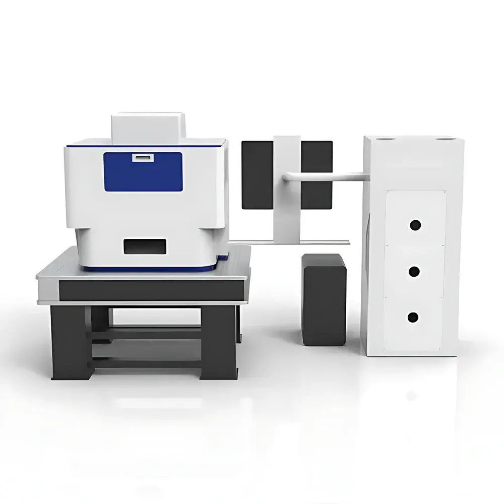
The Abner ABN-WAFER-001 Fully Automated Wafer-Level Transfer Stage is an engineered solution for high-precision, repeatable handling of semiconductor wafers in research, pilot-line, and microfabrication environments. Designed around a robust multi-axis motorized architecture, the system implements precise X/Y/Z/θ motion control combined with vacuum-based wafer immobilization and vision-assisted alignment algorithms. Its core operational principle relies on closed-loop stepper motor actuation with sub-micron step resolution and calibrated position feedback—enabling deterministic placement across process steps such as photolithography, thin-film deposition, etching, metrology, and heterogeneous integration. Unlike manual or semi-automated handlers, the ABN-WAFER-001 executes end-to-end transfer sequences without operator intervention, minimizing mechanical stress, particle generation, and positional drift—critical factors in maintaining cleanroom compatibility and process fidelity.
Key Features
- Multi-Degree-of-Freedom Motion Control: Integrated X/Y linear stages with Z-lift and θ-rotation axes deliver coordinated positioning within ±25 mm travel range (X/Y), 0–160 mm vertical lift, and angular adjustment for fine registration.
- Vacuum-Based Wafer Immobilization: Uniform negative-pressure suction pads ensure non-contact, low-stress adhesion across 2–8 inch wafers—eliminating mechanical clamping-induced deformation, edge chipping, or surface contamination.
- Optical Alignment Capability: Supports automated fiducial or edge-detection alignment via external machine vision systems (e.g., integrated CCD/CMOS cameras), enabling sub-100 µm overlay accuracy between successive process stations.
- Modular & Scalable Architecture: Mechanical and electrical subsystems—including vacuum manifolds, motor drivers, and thermal modules—are decoupled for field-reconfigurable integration with lithography steppers, PVD/CVD tools, or inline inspection platforms.
- Dual-Mode Operation: Equipped with both touchscreen HMI and PC-based software control; supports manual jog, script-driven batch execution, and remote orchestration via LabVIEW APIs or industrial PLC protocols (Modbus RTU over RS-232).
- Comprehensive Safety Interlocks: Real-time monitoring of vacuum pressure, stage limits, motor current, and thermal status triggers fail-safe halts and diagnostic logging—fully compliant with ISO 13857 and IEC 61508 functional safety principles.
Sample Compatibility & Compliance
The ABN-WAFER-001 accommodates standard silicon, sapphire, SiC, and SOI wafers from 50 mm (2″) to 200 mm (8″) diameter. Its vacuum chuck design conforms to SEMI E19-0203 specifications for flatness preservation during handling. While not certified to SEMI S2/S8 out-of-the-box, the system’s mechanical construction, grounding topology, and ESD-safe materials meet baseline requirements for Class 100–1000 cleanroom deployment. All firmware and motion control logic are traceable per GLP-compliant audit trails when operated under validated LabVIEW runtime environments. Optional TCM heating module complies with ASTM E2550 for controlled thermal ramping up to 350 °C—suitable for polymer-assisted transfer processes used in 2D material heterostructure assembly.
Software & Data Management
Control is executed through Abner’s proprietary WaferLink™ software suite (Windows 10/11 compatible), offering GUI-based path programming, parameter versioning, and execution logging with timestamped metadata (position, vacuum level, temperature, error codes). The platform exposes native LabVIEW VIs and Modbus TCP/RTU registers for seamless integration into factory automation frameworks. All motion profiles, alignment offsets, and thermal ramps are stored in encrypted XML configuration files—supporting revision control, multi-user permissions, and FDA 21 CFR Part 11–compliant electronic signatures when deployed with third-party validation packages. Data export supports CSV, HDF5, and industry-standard SECS/GEM message formats for MES connectivity.
Applications
- Semiconductor pilot-line automation: inter-process wafer transport between mask aligners, spin coaters, and plasma etchers.
- Van der Waals heterostructure fabrication: precise stacking of graphene, h-BN, and TMDC monolayers on target substrates using thermal release tape-assisted transfer.
- In-situ metrology staging: positioning wafers under optical microscopes, Raman spectrometers, or AFM systems with micron-level repeatability.
- Advanced packaging R&D: die-to-wafer and wafer-to-wafer alignment for hybrid bonding development.
- University cleanroom labs: standardized wafer handling infrastructure for teaching microfabrication workflows and reproducible device prototyping.
FAQ
Does the ABN-WAFER-001 support integration with third-party vision systems?
Yes—standard GigE Vision and USB3 Vision interfaces allow synchronization with off-the-shelf industrial cameras; calibration routines for pixel-to-micron mapping are included in WaferLink™.
What vacuum level is required for reliable 8-inch wafer handling?
A minimum of −60 kPa (gauge) is recommended; the system includes an integrated diaphragm pump with adjustable pressure regulation and real-time analog feedback.
Can the stage operate inside a nitrogen-purged glovebox?
Yes—the electronics housing meets IP54 ingress protection, and all lubricants and seals are compatible with inert atmospheres; optional stainless-steel vacuum manifold available.
Is thermal expansion compensated during heated transfers?
The TCM heating module includes dual-point PT100 sensors and PID-controlled thermal zoning; software applies empirical thermal drift correction based on pre-characterized wafer-substrate coefficient mismatches.
What documentation is provided for IQ/OQ validation?
Factory test reports, mechanical drawings, firmware checksums, and a URS-aligned validation protocol template are delivered with each unit—supporting GMP-aligned qualification under ISO 9001 and ISO/IEC 17025 frameworks.


