Abner ABN-XRF-001 Wavelength Dispersive X-Ray Fluorescence Spectrometer
| Brand | Abner |
|---|---|
| Origin | Jiangsu, China |
| Model | ABN-XRF-001 |
| Instrument Type | Benchtop |
| Scanning Mode | 2D Mapping |
| Scan Speed | ≤1 frame/sec |
| Detector | 2048 × 2048 CMOS |
| Effective Detection Area | 4.6 mm × 4.6 mm |
| Spatial Resolution | ≤2 µm |
| Quantitative Accuracy | ±0.5% relative error (for major/majority elements) |
| Elemental Range | Na (Z=11) to U (Z=92) |
| Sample Stage Max Size | 30 mm × 30 mm |
| Operating Temperature Range | −196 °C to 100 °C |
| Power Consumption | ≤100 W |
| Safety Compliance | IEC 61010-1, IEC 62471 (UV/X-ray emission limits) |
Overview
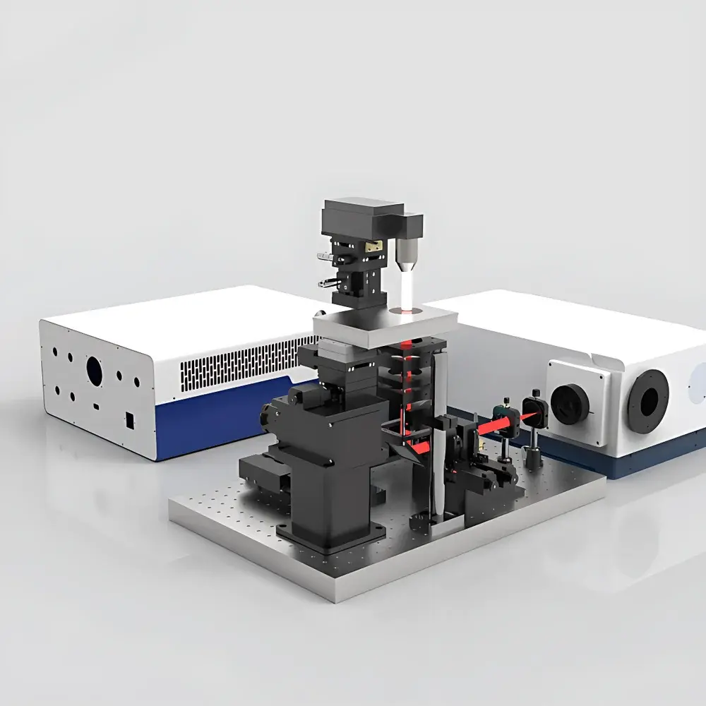
The Abner ABN-XRF-001 is a benchtop wavelength dispersive X-ray fluorescence (WDXRF) spectrometer engineered for high-resolution elemental mapping and quantitative multi-element analysis of solid and thin-film samples. Unlike energy dispersive (EDXRF) systems, the ABN-XRF-001 employs crystal-based wavelength dispersion—using Bragg diffraction from precisely aligned analyzing crystals—to isolate characteristic X-ray lines with superior peak-to-background ratios and spectral resolution. This architecture enables accurate separation of overlapping Kα and Lα lines (e.g., S Kα / Pb Mα, Cr Kα / Fe Kβ), critical for trace-level quantification in complex matrices such as semiconductor wafers, alloy coatings, and geological specimens. The instrument operates on the fundamental principle of primary X-ray excitation inducing inner-shell electron ejection; subsequent relaxation emits element-specific fluorescent X-rays, whose wavelengths are measured via sequential or simultaneous scanning optics. Designed for laboratory-based quality assurance, regulatory compliance testing, and academic research, the ABN-XRF-001 delivers non-destructive, matrix-corrected quantification without sample digestion or vacuum requirements for most applications.
Key Features
- High spatial resolution elemental mapping: ≤2 µm lateral resolution enabled by micro-focused X-ray beam optics and precision motorized stage control
- Benchtop form factor with integrated shielding: Compact footprint (650 × 400 × 550 mm) meets ISO 20487 space requirements for QC labs; lead-lined enclosure complies with IEC 61010-1 Class I safety standards
- CMOS-based position-sensitive detector: 2048 × 2048 pixel array with 4.6 mm × 4.6 mm active area provides high dynamic range and low-noise spectral acquisition
- Real-time 2D scanning capability: Full-frame spectral mapping at ≤1 second per frame supports rapid screening of heterogeneous samples (e.g., inclusion distribution in metallurgical cross-sections)
- Thermostatically controlled sample environment: Integrated cryo-stage support (down to −196 °C) and heated stage (up to 100 °C) enable temperature-dependent speciation studies and volatile sample stabilization
- Low-power X-ray source: Optimized Rh anode tube with ≤100 W total system power draw reduces operational cost and thermal drift during extended acquisitions
Sample Compatibility & Compliance
The ABN-XRF-001 accommodates flat, solid samples up to 30 mm × 30 mm and thicknesses ≤23.5 mm, including polished metals, fused beads, pressed pellets, thin films on Si/SiO₂ substrates, and environmental filters. It supports direct analysis of air-sensitive materials under inert gas purge (N₂/Ar) via optional chamber modification. Method validation aligns with ASTM E1621 (Standard Guide for XRF Elemental Analysis), ISO 22036 (Soil analysis – XRF determination of elements), and USP / (Elemental impurities in pharmaceuticals). Data integrity safeguards include audit-trail-enabled software compliant with FDA 21 CFR Part 11 requirements for electronic records and signatures, supporting GLP and GMP environments.
Software & Data Management
Control and analysis are performed via Abner XRF Suite v4.2—a Windows-based application supporting both point analysis and hyperspectral mapping workflows. The software implements fundamental parameter (FP) algorithms with matrix correction (e.g., alpha correction, absorption-edge modeling) and supports user-defined calibration curves using certified reference materials (CRMs). Raw spectral data is stored in vendor-neutral STF format; processed maps export as TIFF or DICOM for integration with image analysis platforms (e.g., ImageJ, MATLAB). USB 3.0 interface ensures high-throughput transfer of multi-gigabyte hyperspectral datasets. Batch processing, report generation (PDF/Excel), and spectral library matching (NIST SRM database embedded) are standard.
Applications
- Semiconductor process control: Quantitative depth profiling of dopants (B, P, As) and metallic contaminants (Cu, Ni, Fe) in Si wafers and gate dielectrics
- Metallurgy & coating analysis: Alloy grade verification (e.g., stainless steel 304 vs. 316), plating thickness and composition (Ni/Cr/Zn), and interdiffusion layer characterization
- Geochemical exploration: Multi-element mapping of ore textures (e.g., Cu–Fe–S associations in chalcopyrite), REE distribution in monazite, and trace As/Sb in arsenopyrite
- Environmental compliance: Screening of Pb, Cd, Hg, Cr(VI), and Br in RoHS-compliant electronics, soil digests, and airborne particulate filters
- Academic research: In situ phase evolution studies under thermal cycling, corrosion product identification, and cultural heritage pigment analysis (non-invasive pigment stratigraphy)
FAQ
Does the ABN-XRF-001 require vacuum operation for light element analysis?
No. The instrument utilizes helium flush capability and optimized window transmission to enable reliable detection of Na (Z=11) through F (Z=9) without vacuum pumping.
Can it perform depth-resolved analysis?
Yes—via variable incident angle excitation (15°–65°) combined with FP modeling, enabling non-destructive depth profiling down to ~1–5 µm depending on matrix density and element mass.
Is spectral deconvolution supported for overlapping peaks?
Yes. The software includes constrained least-squares fitting with physically informed line shape models (Voigt profiles) and background subtraction using iterative SNIP algorithm.
What reference materials are recommended for calibration?
Certified NIST SRMs (e.g., 610–617 glass series, 2780a soil, 125c brass), BAM metal alloys, and custom matrix-matched standards prepared in-house.
How is instrument performance verified over time?
Built-in drift correction uses internal Mn Kα reference line; daily QC checks include repeatability assessment on Fe/Ni/Cu ternary standard and resolution verification using Co Kα/Kβ doublet separation.