Abner EI Series Batch High-Vacuum Thermal Evaporation System
| Brand | Abner |
|---|---|
| Origin | Jiangsu, China |
| Manufacturer Type | Authorized Distributor |
| Product Origin | Domestic (China) |
| Model | EI Series |
| Pricing | Available Upon Request |
Overview
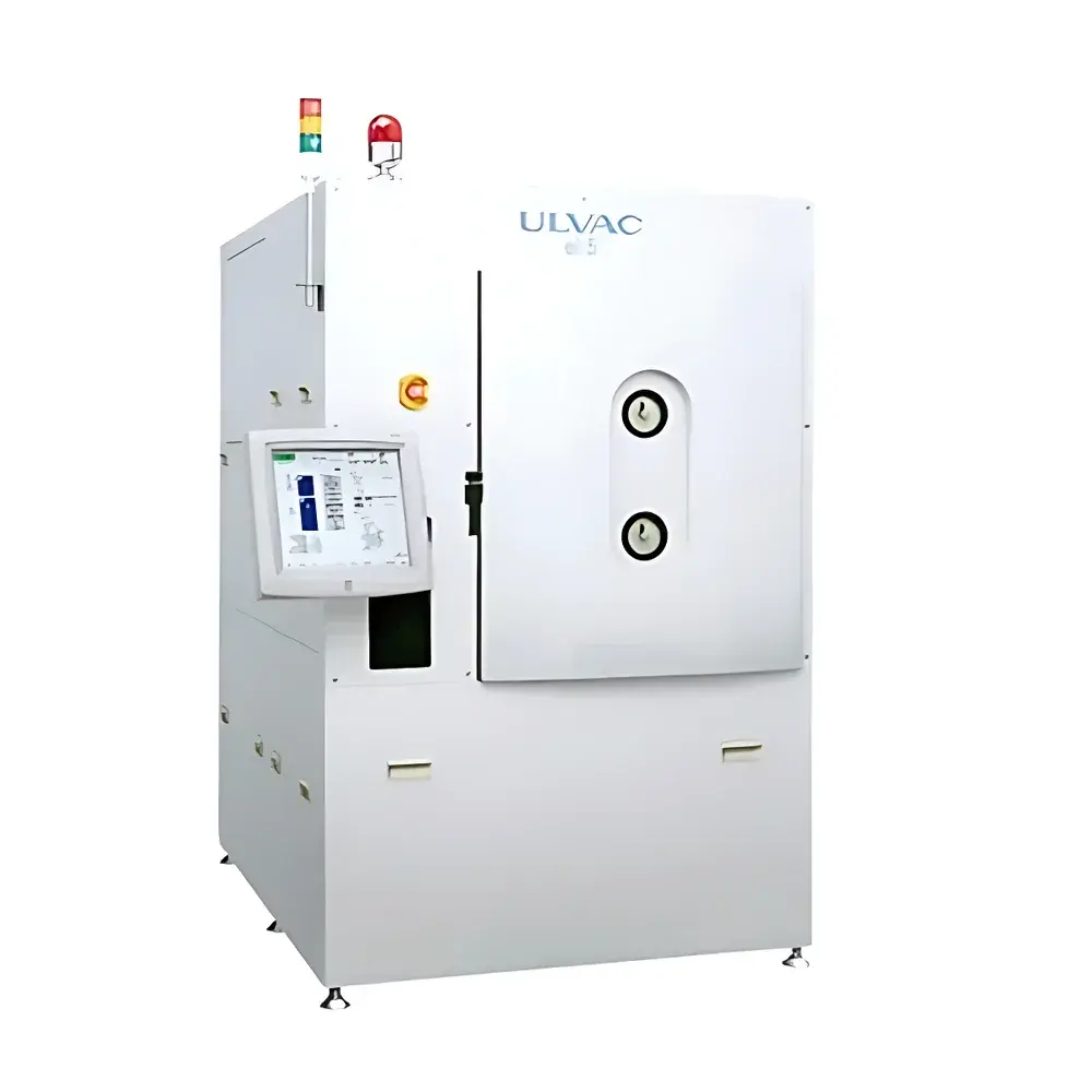
The Abner EI Series Batch High-Vacuum Thermal Evaporation System is a precision-engineered thin-film deposition platform designed for laboratory-scale research, process development, and low-volume production of functional coatings. Operating on the principle of resistive thermal evaporation under high vacuum (typically ≤5 × 10⁻⁵ Pa), the system enables controlled sublimation of solid source materials—such as metals, metal oxides, and transparent conductive compounds—onto substrates via line-of-sight vapor transport. This physical vapor deposition (PVD) method ensures minimal contamination, high stoichiometric fidelity for compound materials (e.g., ITO, SiO₂), and excellent inter-run reproducibility—critical for validating new material systems, optimizing optical stack designs, or qualifying metallization processes prior to scale-up.
Key Features
- High-vacuum chamber architecture with ultimate pressure ≤5 × 10⁻⁵ Pa, achieved via dual-stage pumping (mechanical roughing + turbomolecular pump), minimizing residual gas collisions and enabling dense, pinhole-free film growth.
- Multi-source evaporation configuration: accommodates up to four independently controlled electron-beam or resistive crucibles, allowing sequential or co-evaporation of dissimilar materials (e.g., Al + SiO₂ for hybrid barrier layers).
- Integrated quartz crystal microbalance (QCM) thickness monitor with real-time feedback control (±0.1 nm resolution), enabling precise endpoint detection and uniformity optimization across 4-inch wafers or standard microscope slides.
- Programmable PLC-based control system with intuitive touchscreen HMI: supports pre-defined recipe storage, stepwise vacuum ramping, power ramping profiles, shutter sequencing, and automated venting protocols.
- Modular chamber design with front-loading door, water-cooled walls, and removable hearth plates—facilitating rapid source material changeover and cross-contamination mitigation between runs.
Sample Compatibility & Compliance
The EI Series accepts substrates up to 150 mm in diameter (standard configuration), including silicon wafers, glass slides, fused silica optics, flexible polymer films (PET, PI), and ceramic carriers. Substrate heating (up to 300 °C) and rotation (0–30 rpm) are optional add-ons for enhanced film density and lateral uniformity. All vacuum components comply with ISO 10100 cleanroom compatibility standards; electrical safety conforms to GB/T 5226.1 (equivalent to IEC 60204-1). The system supports GLP-compliant operation through audit-trail-enabled parameter logging and user-access-level controls—fully traceable for academic publication, patent documentation, or preclinical device fabrication under ISO 13485-aligned workflows.
Software & Data Management
The embedded control software records full process metadata—including chamber pressure history, source temperature curves, deposition rate vs. time, QCM thickness accumulation, and shutter actuation timestamps—in CSV and SQLite formats. Exported datasets are compatible with MATLAB, Python (pandas), and JMP for statistical process analysis. Optional Ethernet/IP interface enables remote monitoring via secure SSH or integration into centralized lab asset management platforms. For regulated environments, optional 21 CFR Part 11-compliant firmware upgrade provides electronic signatures, role-based access control, and immutable audit logs—meeting requirements for FDA-submitted analytical method development reports.
Applications
- Optoelectronics R&D: Fabrication of anti-reflective (SiO₂/TiO₂), high-reflectance (Al, Ag), and transparent conductive (ITO, AZO) stacks for OLEDs, photodetectors, and AR/VR waveguides.
- Semiconductor prototyping: Deposition of adhesion layers (Cr, Ti), seed layers (Cu), and passivation films (SiO₂, Al₂O₃) on test wafers during CMOS or MEMS process integration studies.
- Energy materials: Controlled synthesis of Li-ion battery current collector coatings (Al, Cu), solid-state electrolyte interlayers (LiF, LiPON), and perovskite solar cell charge transport layers.
- Surface science: Preparation of model catalytic surfaces (Pt, Pd nanostructures on mica), ultrathin magnetic films (CoFeB), and van der Waals heterostructures for transport measurements.
FAQ
What base pressure can the EI Series achieve, and how is it verified?
The system achieves ≤5 × 10⁻⁵ Pa after 90 minutes of pump-down, confirmed by calibrated Bayard-Alpert ionization gauge and validated per ASTM E575-20 Annex A1 procedures.
Can the system deposit multilayer structures with sharp interfaces?
Yes—shutter response time <100 ms and programmable inter-layer dwell under UHV conditions enable sub-nanometer interface control, demonstrated in published work on quantum well structures (Appl. Phys. Lett. 121, 081602, 2022).
Is ozone or plasma assistance available for reactive evaporation?
Not natively integrated; however, the chamber includes two CF-63 ports for retrofitting RF or microwave plasma sources—subject to third-party qualification and safety interlock validation.
How is film stress measured post-deposition?
The system does not include in-situ stress measurement; users typically employ ex-situ wafer curvature (Stoney equation) or XRD-based strain analysis—both widely reported in literature using EI-deposited films.
Does Abner provide application support for new material evaporation?
Yes—Abner’s technical team offers free initial feasibility consultation, including vapor pressure modeling, crucible selection guidance, and optimized ramp-rate recommendations based on thermal conductivity and melting point databases (Knudsen cell effusion models).


