Abner WT-Series Wafer Transfer Stage
| Brand | Abner |
|---|---|
| Origin | Jiangsu, China |
| Manufacturer Type | Authorized Distributor |
| Product Category | Domestic |
| Model | WT-Series |
| Price | USD 35,000 (FOB Jiangsu) |
| Product Type | Manual Translation Stage |
| Wafer Compatibility | 2–8 inch |
| Motion Axes | X/Y/Z/θ (motorized) |
| Vacuum Chuck | Uniform negative-pressure adsorption |
| Positioning Accuracy | ≤0.1 mm |
| Step Resolution | ≤2 µm |
| Max Load | 4 kg |
| Vertical Travel Range | 0–160 mm |
| Heating Option | TCM-heated platform (up to 350 °C) |
| Control Interface | USB, RS-232, touchscreen HMI |
| Software Support | LabVIEW, PLC, X-BOX remote protocol |
| Operating Temp | 0–80 °C |
| Humidity | ≤80% RH |
Overview
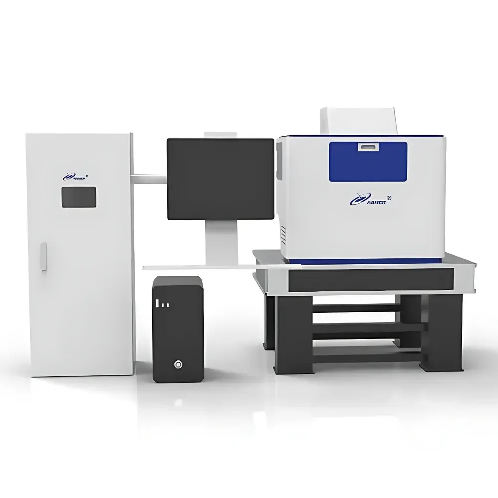
The Abner WT-Series Wafer Transfer Stage is a precision-engineered optical translation stage designed for semiconductor R&D, micro/nano-fabrication, and advanced materials integration. Unlike standard manual translation stages, the WT-Series integrates motorized multi-axis motion control (X/Y/Z/θ), vacuum-based wafer handling, and optical alignment capability—making it suitable for both research-grade automation and pilot-line process bridging. Its core operational principle relies on coordinated piezoelectric or stepper-motor-driven linear and rotational motion, coupled with vacuum-assisted clamping to ensure mechanical stability without surface contact stress. This architecture enables repeatable sub-0.1 mm positioning accuracy across 2–8 inch wafers—critical for mask alignment in lithography, layer-to-layer registration in heterostructure transfer, and sequential processing in vacuum-integrated tool clusters. The system operates within Class 1000 cleanroom-compatible environmental envelopes and is engineered for long-term thermal and mechanical stability under variable load conditions.
Key Features
- Motorized 4-axis motion control (X/Y/Z/θ) with ≤2 µm step resolution and ≤0.1 mm absolute positioning accuracy
- Uniform vacuum chuck system with distributed suction ports—eliminates localized stress, surface scratching, or particle generation during handling
- Optical alignment module supporting edge detection and fiducial mark recognition for automated wafer registration
- Modular quick-change adapter plates for rapid reconfiguration between 2″, 4″, 6″, and 8″ wafer formats
- Integrated TCM-heated platform option (max. 350 °C) with closed-loop temperature feedback for thermally assisted transfer processes
- Touchscreen HMI with dual-mode operation: manual jog control and script-based automated sequence execution
- Multi-protocol communication interface (USB 2.0, RS-232, and optional Ethernet) enabling seamless integration with LabVIEW, PLC, and third-party equipment controllers
Sample Compatibility & Compliance
The WT-Series accommodates silicon, SOI, sapphire, quartz, and 2D-material-coated wafers ranging from 50 mm (2″) to 200 mm (8″) in diameter. Its vacuum chuck design complies with SEMI F47-0201 standards for pneumatic safety in semiconductor handling equipment. Mechanical construction meets ISO 9001-certified manufacturing protocols, and all electrical subsystems conform to IEC 61000-6-2 (EMC immunity) and IEC 61000-6-4 (EMC emission) requirements. While not classified as GMP-grade hardware, its audit-ready software logs (including timestamped motion events, vacuum status, and error codes) support GLP-compliant documentation workflows in academic and pre-commercial development environments.
Software & Data Management
Control firmware supports deterministic real-time motion sequencing via ASCII command sets over serial/USB. The bundled PC application provides GUI-based path planning, parameter calibration (e.g., backlash compensation, homing offset), and batch script generation. All motion profiles, vacuum activation timestamps, and sensor-triggered events are logged in CSV format with UTC synchronization. For regulated environments, optional LabVIEW drivers include FDA 21 CFR Part 11-compliant electronic signature and audit trail modules—enabling traceability of every positional command issued during material transfer operations.
Applications
- Inter-process wafer transport between photolithography steppers, PVD/CVD chambers, and plasma etch tools in pilot-line integration
- Van der Waals transfer of 2D materials (graphene, TMDs, hBN) onto target substrates with angular registration <0.5°
- Multi-step optical alignment in hybrid integration platforms for photonics and quantum device fabrication
- Automated sample staging in in-situ SEM/TEM transfer holders requiring precise Z-height repeatability
- Customizable mounting interface for integration into laser annealing, Raman mapping, or ellipsometry workstations
FAQ
Is this stage compatible with cleanroom Class 100 environments?
Yes—the vacuum lines use stainless-steel tubing and fluoropolymer seals; all surface finishes meet ISO 14644-1 particle shedding limits for ISO Class 5 (Class 100) when operated with HEPA-filtered air supply.
Can the system be integrated into a fully automated cluster tool?
Yes—RS-232 and USB command sets support SECS/GEM protocol translation via external gateway; full integration documentation and handshake timing diagrams are provided upon request.
Does the vacuum chuck support porous or patterned wafers?
Standard configuration supports continuous-backside wafers; optional custom chuck designs with segmented vacuum zones are available for MEMS wafers or devices with backside trenches.
What is the maximum allowable vibration level during operation?
Mechanical resonance damping ensures RMS vibration <0.5 µm at 1–100 Hz when mounted on granite or active isolation tables per ISO 230-2 Annex B test methodology.
Is firmware update capability supported remotely?
Yes—field-upgradable firmware via USB mass storage mode; version history and checksum verification included in release packages.


