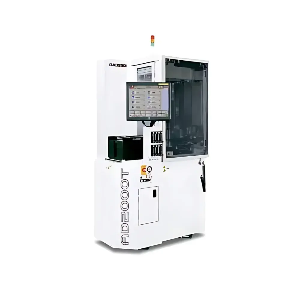
Accretech AD2000TS Precision Wafer Slicing Machine
| Brand | Accretech |
|---|---|
| Origin | Japan |
| Model | AD2000TS |
| Equipment Type | Semiconductor Wafer Slicing System |
| Application Domain | Silicon Wafer Dicing & Kerfless Slice Separation |
| Compliance Context | Designed for ISO 14644-1 Class 5 Cleanroom Integration |
| Control Architecture | CNC-based Closed-loop Motion Control with Real-time Vibration Damping |
Overview
The Accretech AD2000TS is a high-precision, CNC-controlled wafer slicing machine engineered specifically for the semiconductor industry’s demanding requirements in silicon wafer preparation. Unlike conventional dicing saws or mechanical cleavage tools, the AD2000TS employs a hybrid blade-and-stress-assisted separation methodology—combining ultra-thin diamond-impregnated blade cutting with controlled mechanical stress application to minimize subsurface damage and achieve sub-micron kerf loss. Its core architecture integrates a high-rigidity granite base, air-bearing Z-axis motion stage, and real-time force feedback during blade engagement—enabling consistent slice thickness control across 100 mm to 300 mm diameter wafers (including SOI and compound semiconductor substrates such as SiC and GaN). The system is purpose-built for front-end wafer prep workflows where dimensional stability, edge chipping reduction (<0.5 µm), and surface integrity preservation are critical prior to epitaxial growth or device fabrication.
Key Features
- Granite structural frame with integrated vibration isolation—designed to maintain positional repeatability within ±0.3 µm over extended operational cycles
- CNC-driven dual-axis motion system (X/Y) with linear motor drives and optical encoder feedback (resolution: 0.1 µm)
- Adjustable blade spindle capable of rotational speeds from 1,000 to 12,000 rpm, optimized for both resin-bonded and metal-bonded diamond blades
- Real-time cutting force monitoring via piezoelectric load cells—enabling adaptive feed rate modulation to prevent wafer fracture during high-aspect-ratio slicing
- Integrated coolant delivery manifold with temperature-stabilized deionized water flow (±0.2°C) to suppress thermal drift and suppress particle generation
- Modular chuck design supporting vacuum and electrostatic clamping configurations—compatible with carrier-bonded and free-standing wafers up to 2 mm thickness
Sample Compatibility & Compliance
The AD2000TS accommodates standard semiconductor wafer formats including 100 mm, 150 mm, 200 mm, and 300 mm diameters, with optional adapters for non-standard geometries (e.g., rectangular SiC substrates). It supports monocrystalline silicon, fused silica, sapphire, and wide-bandgap materials—provided appropriate blade selection and process parameters are applied. From a regulatory standpoint, the system is engineered for integration into ISO/IEC 17025-accredited laboratories and complies with SEMI S2-0215 (safety) and SEMI E10-0217 (defect classification) guidelines. Its mechanical design meets CE Machinery Directive 2006/42/EC requirements, and electrical subsystems conform to IEC 61000-6-2/6-4 immunity and emission standards. While not inherently 21 CFR Part 11 compliant, its optional data logging module supports audit-trail-ready operation when deployed under GLP/GMP quality systems.
Software & Data Management
Operation is managed through Accretech’s proprietary SliceControl™ v4.2 software suite—installed on an industrial-grade embedded PC with deterministic real-time OS. The interface provides full parametric mapping of blade wear compensation, depth-of-cut profiling, and multi-pass slicing sequences with automatic tool offset recalibration. All process logs—including spindle current, Z-force transients, coolant pressure, and stage position traces—are timestamped and exportable in CSV or HDF5 format. Optional integration with factory MES platforms (via OPC UA 1.04) enables traceability linkage to lot ID, wafer map coordinates, and post-process metrology results. Raw sensor streams can be archived for root-cause analysis during yield excursions or failure mode investigations.
Applications
- Precision slicing of ingots into prime wafers prior to lapping and polishing
- Kerf-loss minimization in photovoltaic-grade silicon wafer production
- Preparation of thin-film SOI substrates with controlled handle layer thickness
- Segmentation of GaN-on-silicon epiwafers for power device fabrication
- Research-scale cleaving of novel 2D material heterostructures bonded to carrier wafers
- Process development for laser-assisted stealth dicing hybrid workflows
FAQ
What wafer thicknesses can the AD2000TS accommodate?
Standard configuration supports wafers from 200 µm to 2 mm thick; custom chucks extend capability to 5 mm for specialized crystal growth substrates.
Is blade auto-dressing supported?
Yes—the system includes programmable dressing cycles synchronized with spindle rotation and feed velocity, compatible with diamond dressers meeting SEMI F57 specifications.
Can the AD2000TS be integrated into an automated wet bench line?
It features SECS/GEM communication protocol support and mechanical interlock interfaces compliant with SEMI E30-0703, enabling seamless handoff to downstream cleaning or inspection stations.
Does the system provide traceable calibration documentation?
Each unit ships with NIST-traceable calibration certificates for position encoders, force sensors, and coolant temperature sensors—valid for 12 months under standard operating conditions.
What maintenance intervals are recommended for sustained precision?
Preventive maintenance is scheduled every 1,000 operational hours or 12 months (whichever occurs first), focusing on air bearing clearance verification, spindle preload adjustment, and coolant filtration system replacement.


