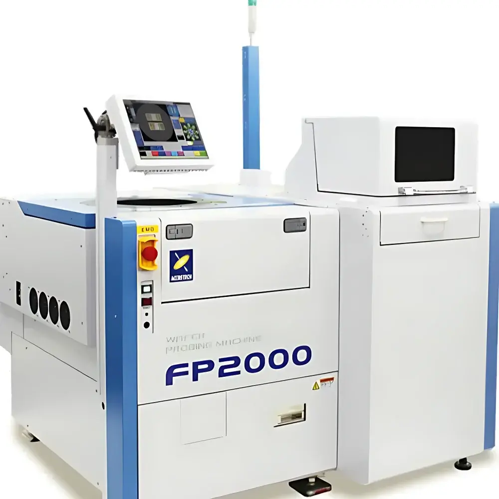
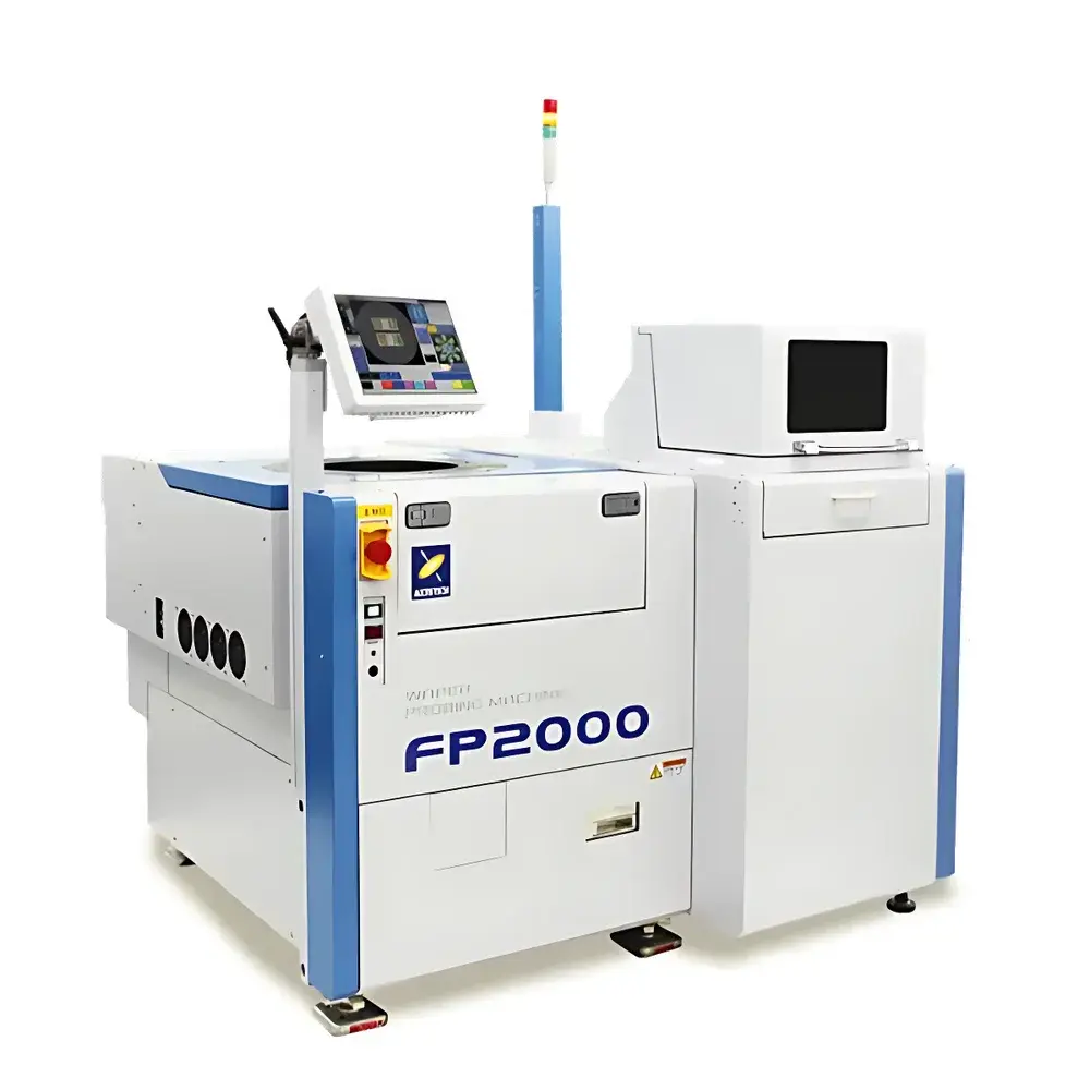
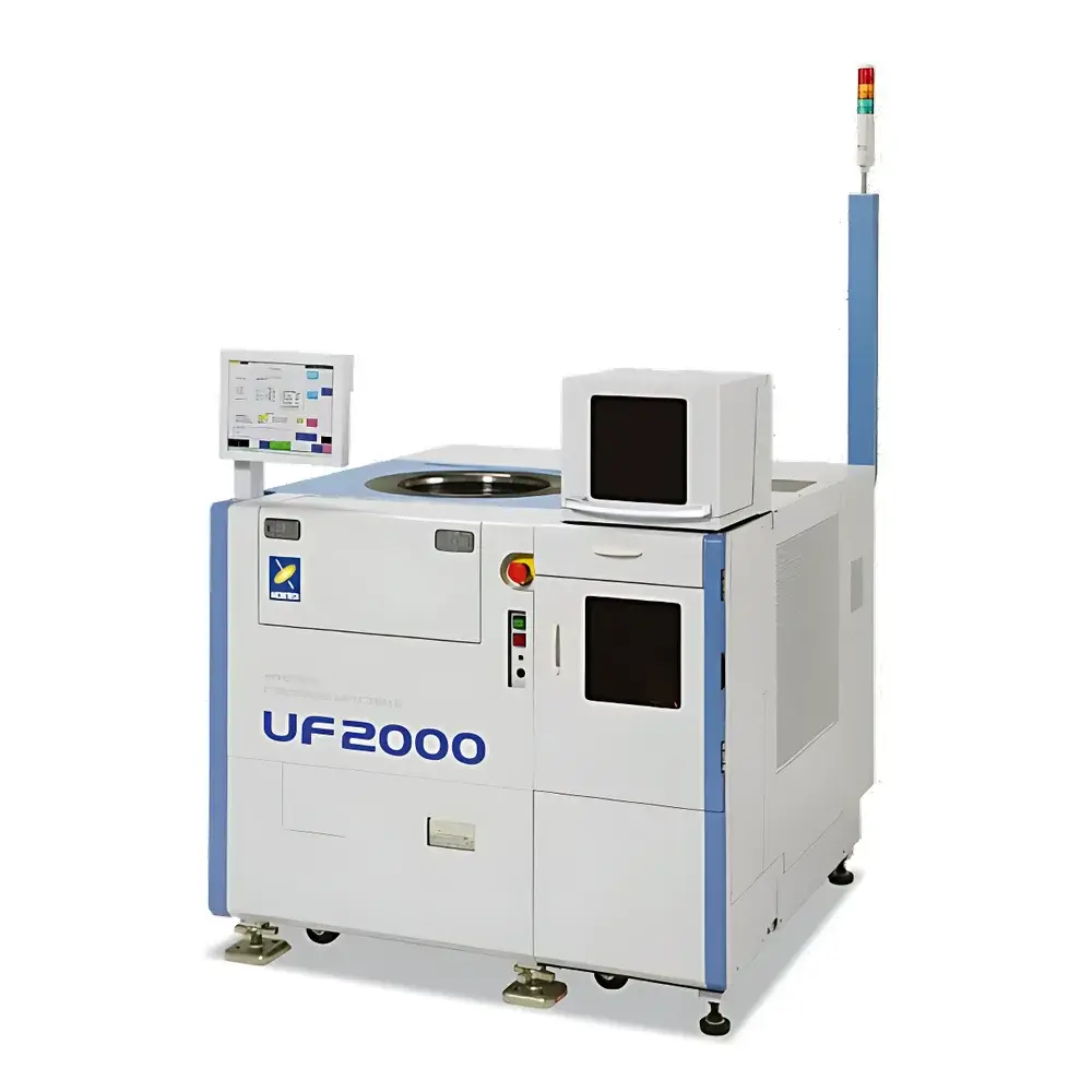
ACCRETECH Fortia Series Fully Automated Probe Station for 200mm Power Devices
| Brand | ACCRETECH (Tokyo Seimitsu) |
|---|---|
| Origin | Netherlands |
| Model | Fortia |
| Wafer Size Support | Φ200 mm |
| Application Focus | DC High-Current/High-Voltage, Avalanche (L-Load), and Wide-Temperature Range Characterization of Power Devices |
| Temperature Range | -65 °C to +300 °C (configurable) |
| Probe Card Compatibility | Up to 330 mm² PLP (Probe Landing Pad) |
| Interface Standards | GEM/SECS-II, TCP/IP, GB-IB, VegaNet |
| Motion Control | Integrated ATi Unit (ACCRETECH TESEC Interface) with DARUMA Stage and Pressurized Chuck |
| Safety Features | Fast Path Interruption during Avalanche Testing, Fault-Triggered Electrical Isolation |
Overview
The ACCRETECH Fortia Series Fully Automated Probe Station is an engineered solution for high-fidelity electrical characterization of discrete power semiconductor devices on 200 mm wafers and diced frames. Designed specifically for demanding DC, transient, and avalanche stress testing—including high-current (>100 A), high-voltage (>3 kV), and L-load (inductive turn-off) measurements—the Fortia integrates precision mechanical alignment, thermally stable chucking, and real-time fault-responsive safety architecture. Its measurement principle relies on controlled probe-to-pad contact under programmable force, synchronized with external parametric test systems (e.g., Keysight B1500A, Teradyne UltraFLEX) via standardized semiconductor equipment communication protocols (GEM/SECS-II). Unlike general-purpose probe stations, the Fortia embeds application-specific hardware layers—such as the ATi (ACCRETECH TESEC interface) unit, DARUMA high-precision XY stage, and pressurized vacuum chuck—to ensure repeatable contact resistance (<5 mΩ typical), minimal thermal drift (<±0.1 °C over 2 hrs at 200 °C), and sub-micron positional reproducibility. It supports full process integration in both wafer-level reliability screening (WAT) and final qualification (Final Test), aligning with JEDEC JESD22-A108 and AEC-Q101 requirements for power device validation.
Key Features
- Wide thermal operating range: programmable from –65 °C to +300 °C using integrated liquid-nitrogen-cooled or resistive-heated chuck modules, with active temperature uniformity control (±0.5 °C across 200 mm)
- ATi interface unit enabling direct synchronization with TESEC, Advantest, and Keysight test platforms—eliminating external trigger latency and supporting real-time pass/fail feedback loops
- DARUMA high-rigidity XY stage with <100 nm step resolution and <±0.3 µm repeatability over full travel (220 × 220 mm), optimized for multi-site probing of trench-gate IGBTs and SiC MOSFETs
- Pressurized vacuum chuck system with dual-zone pressure control (edge + center) to accommodate warped or ultra-thin (<50 µm) wafers without slippage or micro-fracture
- Fast electrical path interruption (<50 µs) triggered by overcurrent, overvoltage, or thermal runaway events—compliant with IEC 61000-4-5 surge immunity and UL 61010-1 functional safety guidelines
- Modular option architecture: configurable RF shielding, low-noise preamp integration, HV guard ring fixtures, and POGO-pin-based parallel probing for 12-device simultaneous characterization
Sample Compatibility & Compliance
The Fortia accommodates 200 mm wafers (flat or notch), diced frames (up to 150 × 150 mm), and discrete packages (TO-247, D2PAK, LFPAK). It supports manual and AMHS-integrated loading via dual-loadport configuration. All motion and environmental subsystems comply with SEMI E10 (Specification for Definition and Measurement of Equipment Reliability and Availability) and SEMI E19 (Equipment Communications Standard). Thermal calibration traceability follows ISO/IEC 17025-accredited procedures. The system meets electromagnetic compatibility (EMC) requirements per CISPR 11 Group 2 Class A and operates within cleanroom Class 100 (ISO 5) environments when equipped with FFU filtration. For regulated production use, audit-ready logging—including probe touchdown force, chuck temperature history, and GEM event traces—is retained for ≥36 months and supports FDA 21 CFR Part 11 electronic signature compliance when paired with validated LIMS interfaces.
Software & Data Management
Control is executed through ACCRETECH’s proprietary ProStation OS v4.2—a deterministic real-time platform built on VxWorks RTOS. The GUI supports script-based recipe automation (Python 3.9 embedded interpreter), cross-platform data export (CSV, HDF5, STDF), and bidirectional mapping with test executive software (e.g., NI TestStand, Advantest TPS). All measurement metadata—including probe card ID (RFID/NFC), wafer map coordinates, thermal soak duration, and contact resistance trend logs—are stored in a relational SQLite database with SHA-256 checksum integrity verification. Remote diagnostics and firmware updates occur via TLS 1.3-secured HTTP/2 channels; no inbound remote desktop access is enabled by default. Audit trails record operator login, parameter changes, and emergency stop events with UTC timestamps and user IDs—fully compliant with GLP and GMP documentation standards.
Applications
The Fortia serves critical roles in power device development and manufacturing: RDS(on), Vth, and gate charge (Qg) extraction across temperature; short-circuit ruggedness evaluation (SCSOA); unclamped inductive switching (UIS) and avalanche energy (EAS) quantification; dynamic RDS(on) tracking during Miller plateau transitions; and long-term HTGB/HTGS bias stability monitoring. It is deployed in foundry process development labs (e.g., for SiC epitaxy optimization), IDMs performing AEC-Q101 qualification, and OSATs executing burn-in correlation studies. Its modular design allows reconfiguration for GaN HEMT gate leakage mapping, superjunction MOSFET body diode recovery analysis, and automotive-grade TVS diode clamping validation.
FAQ
What wafer sizes and form factors does the Fortia support?
It handles 200 mm wafers (with flat or notch), diced frames up to 150 × 150 mm, and discrete packages including TO-220, TO-247, DFN5×6, and LFPAK.
Is the system compatible with third-party parametric testers?
Yes—via GEM/SECS-II, TCP/IP socket, or GB-IB; certified interoperability exists with Keysight, Tektronix, Advantest, and Teradyne platforms.
How is thermal uniformity maintained during high-temperature testing?
Using a dual-zone heated chuck with embedded Pt100 sensors, closed-loop PID control, and edge-compensation algorithms—validated per ASTM E220.
Can the Fortia perform simultaneous multi-device avalanche testing?
Yes—when configured with the optional 12-position POGO tower and ATi-synchronized current sourcing, it enables parallel UIS stress on up to 12 identical dies.
Does the system support automated probe card cleaning and alignment verification?
Integrated optical needle inspection (ONI) provides real-time probe tip imaging and wear analytics; dry nitrogen purge and optional plasma cleaning modules are available as add-ons.


