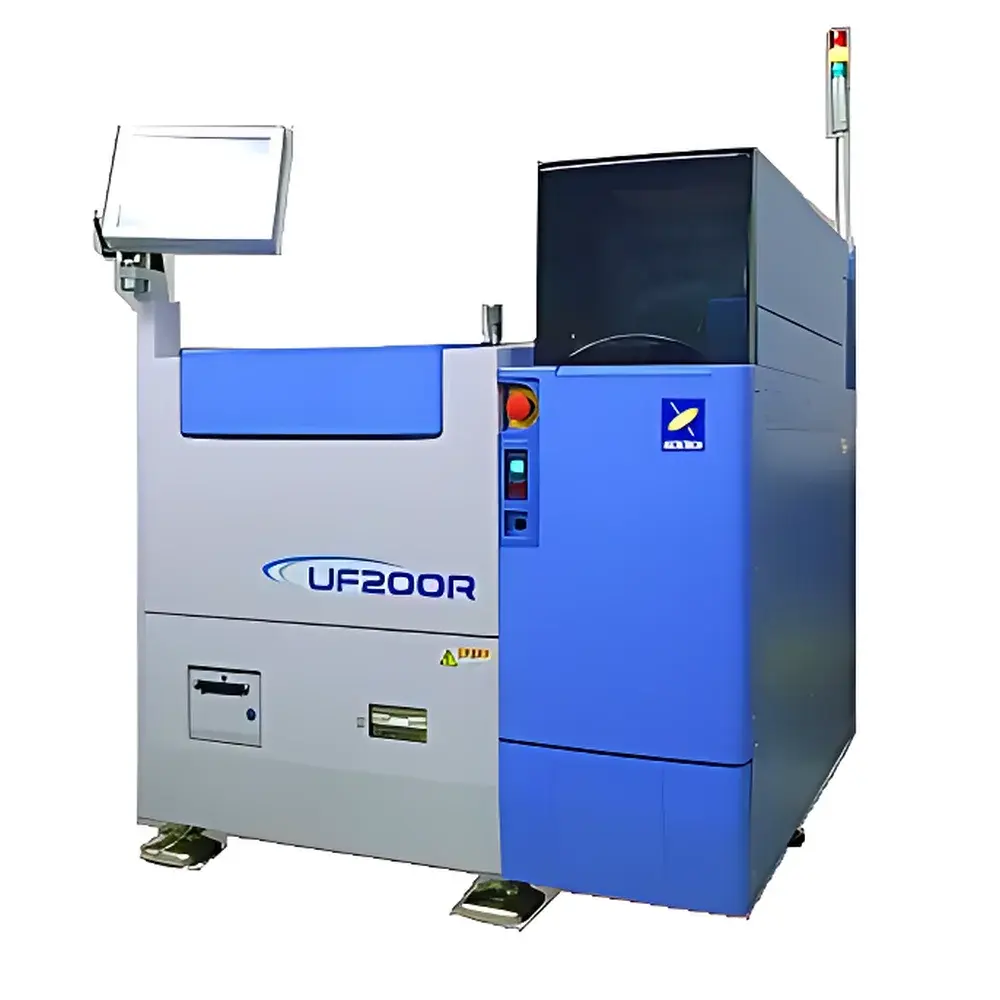
Accretech TSK UF200R Fully Automated RF Probe Station
| Brand | Accretech (ACCRETECH) |
|---|---|
| Origin | Japan |
| Model | UF200R |
| Wafer Size Capacity | 200 mm (8-inch) |
| Automation Level | Fully Automatic |
| Probe Station Type | RF Probe Station |
| Compliance | Designed for ISO Class 5 cleanroom environments |
| Structural Rigidity | High-stiffness chuck with ITV fine alignment system |
| Thermal Operation Range | Up to +150 °C |
| Key Software Capabilities | Inkless wafer mapping, multisite parallel probing, OTS optical auto-alignment |
| Motion Control | Upgraded servo-driven XYZθ stage with sub-micron repeatability |
| Application Domain | LSI/VLSI wafer-level parametric testing, RF device characterization, high-reliability IC qualification |
Overview
The Accretech TSK UF200R Fully Automated RF Probe Station is an engineered upgrade of the proven UF200 platform, developed by Tokyo Seimitsu Co., Ltd. (now part of Accretech Group) and refined for advanced semiconductor wafer-level testing in R&D, process development, and high-mix production environments. Built upon a rigid granite base and precision-machined structural frame, the UF200R employs Couette-flow-optimized motion architecture and low-vibration piezoelectric actuators to ensure mechanical stability during high-frequency RF probing (DC–67 GHz typical, compatible with active probes up to 110 GHz). Its core measurement principle relies on precise physical contact between calibrated RF microprobes and device-under-test (DUT) pads under controlled environmental conditions—enabling accurate extraction of S-parameters, IV curves, noise figure, and transistor gain compression metrics. The system supports full-wafer automation from cassette load/unload through optical pre-alignment, die recognition, probe landing, signal acquisition, and post-test data logging—all without operator intervention.
Key Features
- Optical Targeting System (OTS): Next-generation real-time image-based alignment engine delivering ±0.5 µm positional accuracy across full 200 mm wafer field, with <1.2 s average alignment cycle time per site.
- High-Stiffness Chuck Assembly: Vacuum-compatible ceramic-coated aluminum chuck with integrated thermal control (−55 °C to +150 °C), enabling stable DUT temperature management during extended RF stress tests.
- RF-Optimized Stage Architecture: Dual-stage Z-axis design featuring coarse/fine actuation; fine Z resolution ≤50 nm, repeatability <±0.1 µm over 10⁶ cycles.
- Modular Probe Card Interface: Supports standard 3.5 mm, 2.92 mm, and SMPM RF probe card mounts; mechanically decoupled from stage motion to minimize crosstalk-induced signal distortion.
- Integrated Vibration Isolation: Active pneumatic isolation platform compliant with SEMI S2-0216 vibration class VC-B requirements.
- Firmware-Embedded Safety Protocols: Interlocked emergency stop, probe-overtravel protection, and real-time force monitoring (0.1–500 mN range) to prevent pad damage.
Sample Compatibility & Compliance
The UF200R accommodates standard 200 mm (8-inch) silicon, SiC, GaN, and compound semiconductor wafers—including those with backside metallization or temporary bonding films. It complies with SEMI E10 (Specification for Definition and Measurement of Equipment Reliability and Maintainability), SEMI E142 (Probe Station Performance Test Method), and ISO 14644-1 Class 5 cleanroom operational standards. All motion control firmware and safety logic are certified to IEC 61508 SIL2. For regulated environments, optional audit trail logging and electronic signature modules meet FDA 21 CFR Part 11 and EU Annex 11 requirements when deployed with validated third-party test software (e.g., Cascade Microtech WinCal XE, FormFactor ProberLink).
Software & Data Management
The station runs on a deterministic real-time OS with dual-channel GigE Vision interface for synchronized camera and motion control. Native software includes Accretech’s ProbeStation Suite v4.2—supporting inkless wafer mapping (no physical marking), multisite parallel probing (up to 4 independent probe positions), and automated recipe-based test sequencing. Data export conforms to STDF (Standard Test Data Format) Rev. 5.1 and CSV/JSON schemas compatible with Yield Analysis platforms (e.g., PDF Solutions Exensio, Synopsys Yield Explorer). Optional API integration enables bidirectional communication with MES systems via SECS/GEM protocol stack.
Applications
- Parametric characterization of RF SOI, GaAs pHEMT, and GaN HEMT devices at wafer level.
- High-temperature reliability screening (HTOL, HTRB) for automotive-grade power ICs.
- On-wafer calibration substrate validation (SOLT, TRL) for vector network analyzer traceability.
- Low-noise amplifier (LNA) and power amplifier (PA) linearity analysis (AM-AM/AM-PM, ACPR).
- Process monitor vehicle (PMV) testing across multiple technology nodes (28 nm to 3 nm logic, 65 nm to 0.18 µm analog/RF).
- Failure analysis correlation using synchronized probe position metadata and electrical waveform capture.
FAQ
Does the UF200R support cryogenic probing?
Yes—optional liquid nitrogen or closed-cycle helium cooling modules extend operational range to −65 °C, with thermal gradient control ≤0.5 °C/min and spatial uniformity ±1.2 °C across 200 mm wafer.
Can it integrate with third-party parameter analyzers and VNAs?
Fully supported via SCPI over TCP/IP, IVI-COM drivers, and direct GPIB/LAN interfaces; verified compatibility with Keysight B1500A, Keithley 4200-SCS, and Rohde & Schwarz ZNB series instruments.
Is remote operation and diagnostics available?
Standard Ethernet-based remote desktop access (RDP) and SNMPv3-enabled health monitoring allow predictive maintenance alerts and firmware OTA updates without onsite intervention.
What wafer handling options are available?
Configurable front-end load port (FELP) with SMIF pod or FOUP interface; optional robotic arm integration (SEMI E47-compliant) for cluster tool environments.
How is alignment accuracy verified and maintained?
Built-in NIST-traceable calibration routine uses embedded fiducial targets and multi-point grid verification; annual recalibration recommended per ISO/IEC 17025 accredited service providers.
Related Products


