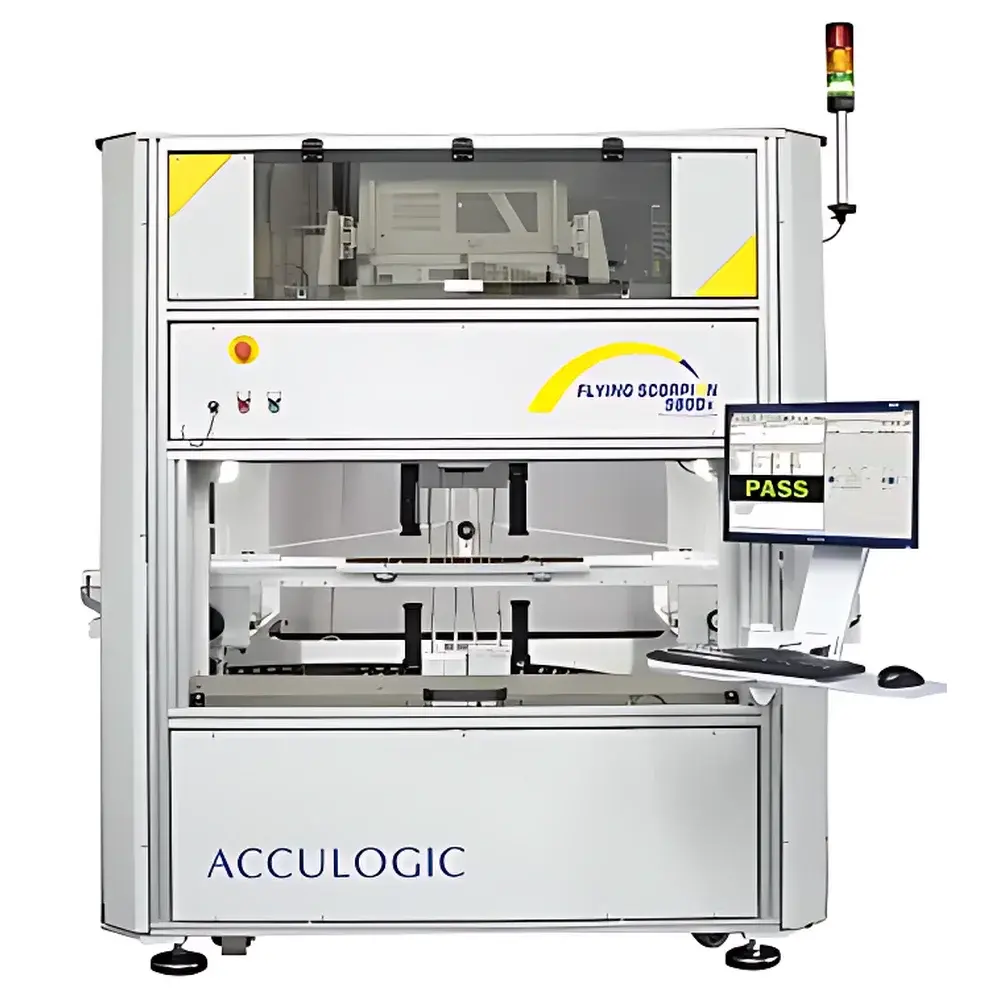
Acculogic FLS980Dxi Flying Probe Test System
| Brand | Acculogic |
|---|---|
| Origin | Canada |
| Model | FLS980Dxi |
| Motion Control | Closed-loop linear motor shuttles |
| Minimum Step Resolution | 1 µm |
| Positioning Repeatability | ±10 µm |
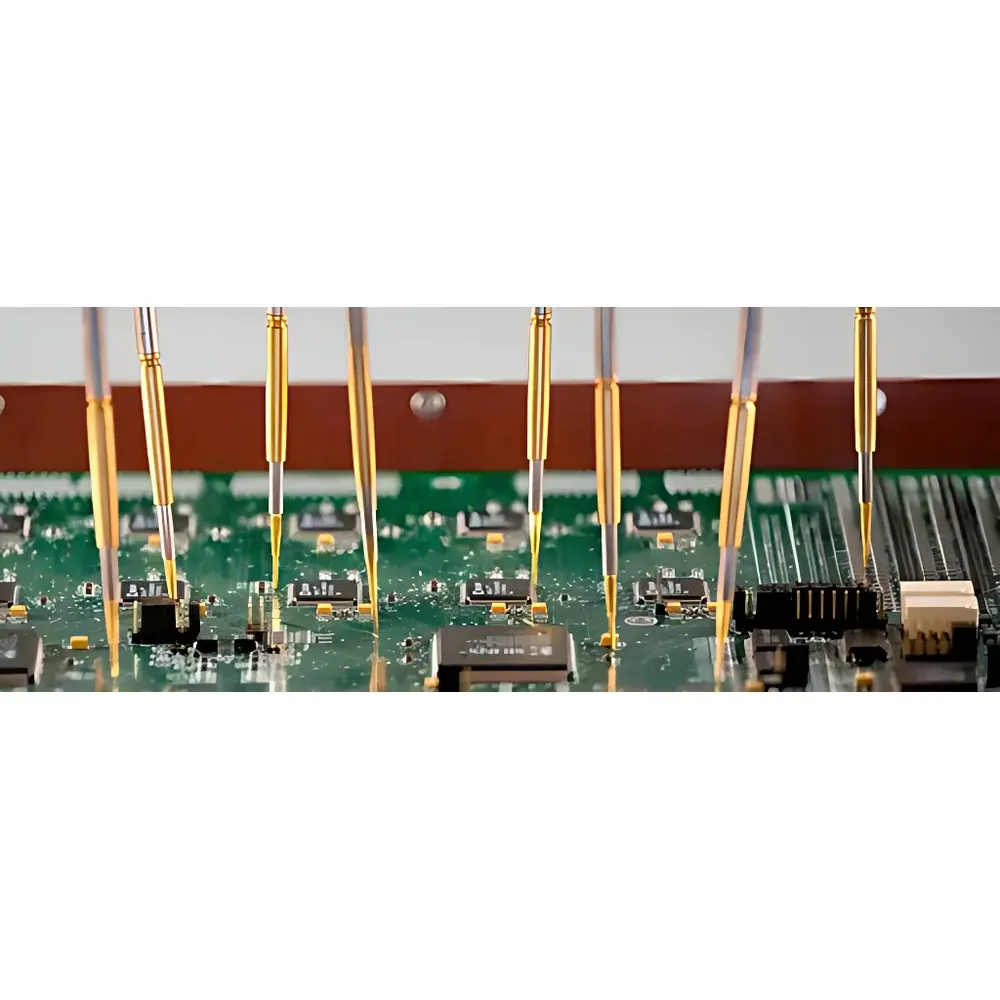
| Maximum Probes | 22 (top + bottom) |
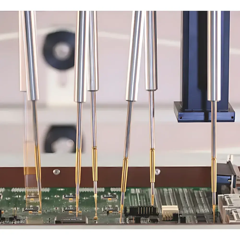
| Programmable Probe Tilt | ±6° |
| PCB Max Size | 813 × 965 mm (32″ × 38″) |
| Max Component Height | 85 mm |
| Max Probe Height | 45 mm |
| Tip Radius Range | 50–500 µm |
| Tip Geometry Options | Needle, Cup, Dome |
| Analog Measurement Speed | Up to 1000 measurements/sec |
| Measurement Modes | 2-wire, 4-wire, quasi-4-wire |
| Stimulus/Measurement Resources | Dual independent channels |
| Supported Test Types | Analog, Digital, Mixed-Signal, Boundary Scan (JTAG), NetScan™ |
| Warpage Compensation | Integrated LaserScan™ and high-res fiducial camera |
| Software Platform | Integrator™ with motion control & measurement algorithms |
| Compliance Framework | Supports GLP/GMP audit trails, ASTM F2627 (for PCB test system validation), ISO/IEC 17025 traceability workflows |
Overview
The Acculogic FLS980Dxi Flying Probe Test System is a high-precision, dual-sided automated test platform engineered for in-circuit testing (ICT) of advanced printed circuit assemblies where traditional bed-of-nails fixtures are impractical or obsolete. Designed specifically for high-mix, low-volume, and prototype-intensive semiconductor and electronics manufacturing environments, the FLS980Dxi employs a closed-loop linear motor shuttle architecture combined with programmable 3D probe modules to achieve sub-10 µm positional repeatability—critical for reliable contact with ultra-miniaturized components such as 01005 passives, fine-pitch QFNs, and chip-scale packages (CSPs). Unlike open-loop flying probe systems, the FLS980Dxi integrates real-time motion feedback at both shuttle and probe actuator levels, eliminating mechanical hysteresis and ensuring deterministic probe placement across thermal and mechanical drift conditions. Its core measurement engine supports simultaneous analog stimulus and response acquisition at up to 1000 samples per second per channel, with full 4-wire Kelvin capability across all 22 probes (11 top / 11 bottom), enabling high-fidelity characterization of low-impedance paths, leakage currents, and parametric device behavior under powered or unpowered conditions.
Key Features
- Closed-loop linear motor shuttles with 1 µm minimum step resolution and ±10 µm positioning repeatability—no mechanical contact, zero friction, and no wear over lifetime operation
- Programmable probe tilt mechanism (±6°) enabling adaptive angle optimization to mitigate warpage-induced misalignment; critical for consistent contact on boards exhibiting >0.3 mm Z-axis deformation
- Dual independent stimulus/measurement resource channels supporting concurrent analog functional testing (e.g., voltage regulator output stability, op-amp gain/offset) and digital boundary-scan (IEEE 1149.1/1687)
- LaserScan™ integrated warpage mapping subsystem co-registered with high-resolution fiducial camera (≥5 MP, telecentric optics) and adaptive illumination for automatic Z-compensation across X-Y test fields up to 813 × 965 mm
- Integrator™ control software featuring deterministic motion planning, real-time probe force monitoring (via piezoresistive feedback), and embedded calibration traceability per ISO/IEC 17025 requirements
- Modular probe head configuration: APM800 (fully programmable tilt), BPM700 (fixed +6°), VPM600 (0° vertical)—allowing mixed deployment optimized for DUT topology and accessibility constraints
Sample Compatibility & Compliance
The FLS980Dxi accommodates PCBs up to 32″ × 38″ (813 × 965 mm) with component heights up to 85 mm and probe access heights up to 45 mm—enabling full coverage of complex multilayer server motherboards, automotive ADAS modules, and RF front-end assemblies. Probe tip geometries (needle, cup, dome) and radii (50–500 µm) are selected based on pad metallurgy, solder mask opening, and reliability requirements—supporting IPC-A-610 Class 3 compliance verification. The system complies with safety standards IEC 61000-6-2 (immunity) and IEC 61000-6-4 (emissions), and its software architecture supports FDA 21 CFR Part 11-compliant electronic signatures, audit trails, and role-based access control when deployed in regulated medical or aerospace production environments. Validation documentation aligns with ASTM F2627 (“Standard Guide for Validation of In-Circuit Test Systems”) and includes factory-certified repeatability reports per probe axis.
Software & Data Management
Integrator™ serves as the unified control, programming, and data management environment for the FLS980Dxi. It provides native support for industry-standard test description formats including STDF, IPC-D-356, and IEEE 1149.1 BSDL files. Test program generation leverages intelligent auto-probing algorithms that analyze netlist topology, component footprints, and physical board geometry to minimize probe travel and optimize test sequence order—reducing average test time by 35–50% versus legacy scripting approaches. All measurement data—including raw analog waveforms, JTAG instruction logs, and LaserScan™ warpage maps—is timestamped, digitally signed, and stored in a structured SQLite-based repository with configurable retention policies. Export interfaces include RESTful APIs for MES integration and CSV/PDF reporting compliant with ISO 9001 clause 8.5.2 (control of nonconforming output).
Applications
The FLS980Dxi is deployed in high-reliability electronics manufacturing for: functional validation of ASIC/FPGA-based control boards prior to burn-in; failure analysis root cause isolation via selective node probing during power-up sequencing; post-reflow solder joint integrity assessment using dynamic resistance trending; reverse engineering support through non-destructive net identification and signal tracing; and qualification of next-generation heterogeneous integration substrates (e.g., silicon interposers, fan-out wafer-level packaging) where conventional fixture-based ICT cannot achieve sufficient probe density or Z-axis clearance. Its GHz-range signal integrity capability (enabled by low-inductance probe cabling and calibrated impedance matching) also supports RF path continuity verification in 5G mmWave front-end modules.
FAQ
What is the maximum board thickness the FLS980Dxi can accommodate?
The system supports PCBs up to 6.5 mm thick when configured with extended Z-axis travel options; standard configuration handles up to 4.2 mm.
Does the system support thermal testing during powered operation?
Yes—optional thermal imaging integration (FLIR Axxx series) enables synchronized IR mapping during functional stimulus, with temperature-triggered test abort logic.
Can probe calibration data be exported for external metrology review?
Yes—calibration certificates, step-response logs, and laser interferometer traceability records are exportable in PDF and XML formats per ISO/IEC 17025 Annex A.3.
Is boundary scan testing limited to JTAG-compatible devices?
No—the system supports IEEE 1149.1, 1149.4 (analog boundary scan), and 1149.6 (AC-coupled interconnect testing) via configurable pin driver/receiver modules.
How is probe wear monitored and compensated?
Real-time piezoresistive force feedback combined with periodic tip geometry verification (via integrated optical profiler) triggers automatic Z-offset recalibration before each test run.


